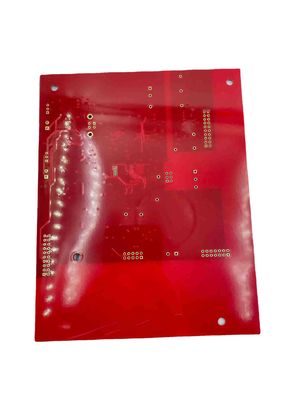
HASL Surface Finish FR4 6 Layer PCB Board Copper Thickness 8OZ

Contact me for free samples and coupons.
Whatsapp:0086 18588475571
Wechat: 0086 18588475571
Skype: sales10@aixton.com
If you have any concern, we provide 24-hour online help.
x| Board Thickness | 3.0mm | Copper Thickness | 8oz |
|---|---|---|---|
| Layer | 6layer | Material | FR4 |
| Min. Hole Size | 0.2mm | Min. Line Spacing | 0.1mm |
| Min. Line Width | 0.1mm | Product Name | Hybrid Circuit Board |
| Silkscreen Color | White | Solder Mask Color | Red |
| Surface Finish | HASL | ||
| Highlight | FR4 6 Layer PCB Board,HASL 6 Layer PCB Board,8OZ Copper FR4 PCB Board |
||
6-layer board thickness 3.0MM copper thickness 8OZ surface spray tin
The board has a thickness of 3.0MM, which is relatively thick compared to standard PCBs. For applications with high current demands or where effective heat dissipation is required
The copper thickness of 8OZ is also relatively thick, and it is often used in applications requiring high power or low resistance.
The board has six layers, allowing for more complex circuit designs and higher component density. A six-layer board can also provide better signal integrity because it allows for more routing options and better separation between signal and power layers.
Surface tin spraying provides a layer of tin on the copper traces to help protect them from corrosion and oxidation. This surface treatment also promotes good solderability, which is important for reliable solder connections.
The combination of thick boards, thick copper layers, and a tin-spray finish indicates that the board is designed for high-power applications that require low resistance and reliable solder connections.
| Item | capability |
| Base Material | FR-4, High TG FR-4 , Halogen Free material ,CEM-3,CEM-1,PTFE,Rogers ,Arlon ,Taconic,Aluminum base,Teflon,PI ,etc |
| Layers | 1-60 |
| Finished inner/outer copper thickness | 0.5-6OZ |
| Finished board thickness | 0.2-7.0mm(≤0.2mm needs review),≤0.4mm for HASL |
| Board thickness≤1.0mm: +/-0.1mm 1Board thickness>2.0mm: +/-8% |
|
| Max panel size | ≤2sidesPCB: 600*1500mm Multilayer PCB: 500*1200mm |
| Min conductor line width/spacing | Inner layers: ≥3/3mil Outer layers: ≥3.5/3.5mil |
| Min hole size | Mechanical hole: 0.15mm Laser hole: 0.1mm |
| Drilling precision: first drilling First drilling: 1mil Second drilling: 4mil |
|
| Warpage | Board thickness≤0.79mm: β≤1.0% 0.80≤Board thickness≤2.4mm: β≤0.7% Board thickness≥2.5mm: β≤0.5% |
| Controlled Impedance | +/- 5 % Ω(<50Ω),+/-10%(≥50Ω),≥50Ω+/-5% (needs review) |
| Aspect Ratio | 15:01 |
| Min welding ring | 4mil |
| Min solder mask bridge | ≥0.08mm |
| Plugging vias capability | 0.2-0.8mm |
| Hole tolerance | PTH: +/-3mil NPTH: +/-2mil |
| Outline profile | Rout/ V-cut/ Bridge/ Stamp hole |
| Solder mask color | Green,yellow,black,blue,red,white,matte green |
| Component mark color | white,yellow,black |
![]()
Shenzhen Jieteng Circuit Co., Ltd. is a trustworthy and reliable PCB manufacturer dedicated to providing high-quality PCBs that meet customers' specific requirements. The company adopts advanced manufacturing equipment and technology, and has a group of experienced engineers and technicians who work closely with customers to ensure that their PCBs are suitable for their needs.
In addition to its commitment to quality, Jeton Circuits Co., Ltd. places great emphasis on customer service. The company works closely with customers to provide individual solutions and support throughout the entire PCB manufacturing process, from design to delivery. This dedication to customer satisfaction has helped the company become a reputable and reliable partner for businesses and organizations requiring high quality PCBs.


