


All Products
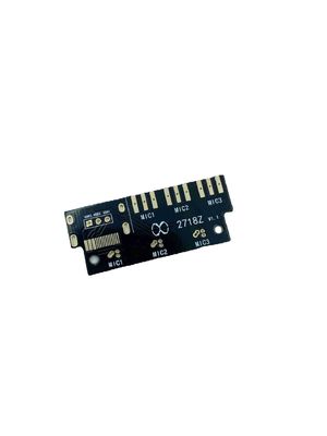
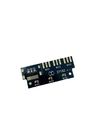
Resin Plugged Hole 4 Layer PCB ENIG Surface 4L Halogen Free 2.0 Thickness

| Place of Origin | china |
|---|---|
| Brand Name | JIETENG |
| Certification | ISO/TS16949/RoHS/TS16949 |
| Model Number | FR4 |
| Minimum Order Quantity | Negotiable |
| Price | Negotiable |
| Packaging Details | Blank carton, vacuum packed |
| Delivery Time | 5-8 working day |
| Payment Terms | Negotiable |
| Supply Ability | 150000 square meters / year |

Contact me for free samples and coupons.
Whatsapp:0086 18588475571
Wechat: 0086 18588475571
Skype: sales10@aixton.com
If you have any concern, we provide 24-hour online help.
xProduct Details
| Base Material | FR4 | Copper Thickness | 1 OZ |
|---|---|---|---|
| Surface Finishing | HASL | Board Thickness | 1.6 |
| Supplier Type | OEM | ||
| Highlight | Resin Plugged Hole 4 Layer PCB,ENIG Surface 4 Layer PCB,Halogen Free Hybrid Circuit Board |
||
Product Description
Resin Plugged Hole 4 Layer PCB ENIG Surface 4L Halogen Free 2.0 Thickness
A resin plugged hole 4 layer PCB is a type of printed circuit board (PCB) that has resin-filled vias or holes that are used to connect the different layers of the PCB. This helps improve the reliability and performance of the PCB by reducing the risk of electrical shorts or opens.
ENIG (Electroless Nickel Immersion Gold) is a type of surface finish applied to the copper traces and pads on the surface of the PCB. It involves depositing a layer of nickel onto the copper, followed by a layer of immersion gold. This finish provides good protection against oxidation and other forms of corrosion, and it is commonly used in high-reliability applications.
A 4-layer PCB has four layers of substrate material and copper traces. This allows for more complex circuit designs and increased functionality compared to single or double-layer PCBs.
Halogen-free refers to the absence of halogens, which are chemicals commonly used in the manufacturing of PCBs that can emit toxic fumes when burned. Halogen-free PCBs are safer for people and the environment, making them a preferred choice for many applications.
2.0 thickness refers to the overall thickness of the PCB. This thickness is usually measured in millimeters and is an important consideration when designing the PCB for specific applications.
| Copper Thickness | 10Z |
| Board Thickness | 2.0MM |
| Min. Hole Size | 0.15mm(mechanical drill) |
| Min. Line Width | 4mil |
| Min. Line Spacing | 4mil |
| Surface Finishing | Customzied |
| Layers | 2 |
| Thicker copper | 1oz |
| Products Types | HDI board |
| Solder mask color | Green Black Red |
| Base meterial | HI-TG |
| Finished Surface | Leed-free HASL |
| Selective Surface Treatment | ENIG(Immersion Gold)+Gold |
| Min Solder Mask Bridge | 0.08mm |
| Aspect ratio | 15:1 |
Shenzhen Jieteng Circuit Co., Ltd. is a Printed Circuit Board (PCB) manufacturer located in Shenzhen, China. Specializing in the production of high-quality PCBs for a wide range of applications including industrial, automotive, telecom and consumer electronics.
The company offers a variety of PCB solutions including single-sided, double-sided and multi-layer PCBs, as well as specialized PCBs for high temperature, high frequency and other demanding applications.
Recommended Products