

All Products
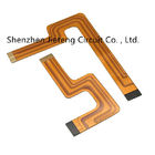
Electronic Component BOM 12 Layer PCB Fabrication And SMD SMT Assembly

| Place of Origin | Guangdong, China |
|---|---|
| Brand Name | JIETENG |
| Certification | ISO/TS16949/RoHS/TS16949 |
| Model Number | PCBA |
| Minimum Order Quantity | Negotiable |
| Price | Negotiable |
| Packaging Details | PCBA Gibson Vaccum packing or Anti-static package Outer:export carton or according to customer's requirement. |
| Delivery Time | 5-10 days for delivery |
| Payment Terms | Negotiable |
| Supply Ability | 80000 Square Meter/Square Meters per Month |

Contact me for free samples and coupons.
Whatsapp:0086 18588475571
Wechat: 0086 18588475571
Skype: sales10@aixton.com
If you have any concern, we provide 24-hour online help.
xProduct Details
| Number Of Layers | 1-48 | Min Solder Mask Clearanace | 0.003"(0.07mm) |
|---|---|---|---|
| Board Thickness | 0.3mm-8mm | Base Material | FR-4,Aluminum,CEM,Hg-170 |
| Highlight | SMD 12 layer pcb fabrication,BOM 12 layer pcb fabrication,BOM smd pcb assembly |
||
Product Description
One-stop electronic component BOM supporting PCB production multi-layer PCB processing production
Essential details
| Article | Description | Capability |
| Material | Laminate materials | FR4, High TG FR4, High Frequency, Alum, FPC... |
| Board Cutting | Number of layers | 1-48 |
| Min.thickness for inner layers (Cu thickness are excluded) |
0.003”(0.07mm) | |
| Board Thickness | Standard | (0.1-4mm±10%) |
| Min. | Single/Double:0.008±0.004” | |
| 4layer:0.01±0.008” | ||
| 8layer:0.01±0.008” | ||
| Bow and twist | no more than 7/1000 | |
| Copper Weight | Outer Cu weight | 0.5-4 0z |
| Inner Cu weight | 0.5-3 0z | |
| Drilling | Min size | 0.0078”(0.2mm) |
| Drill deviation | ±0.002″(0.05mm) | |
| PTH hole tolerance | ±0.002″(0.005mm) | |
| NPTH hole tolerance | ±0.002″(0.005mm) | |
| Solder Mask | Color | Green,white,black,red,blue… |
| Min solder mask clearanace | 0.003″(0.07mm) | |
| Thickness | (0.012*0.017mm) | |
| Silkscreen | Color | white,black,yellow,blue… |
| Min size | 0.006″(0.15mm) | |
| Max Size of Finish Board | 700*460mm | |
| Surface Finish | HASL,ENIG,immersion silver,immersion tin,OSP… | |
| PCB Outline | Square,circle,irregular(with jigs) | |
| Package | QFN,BGA,SSOP,PLCC,LGA | |
![]()
Recommended Products