

All Products
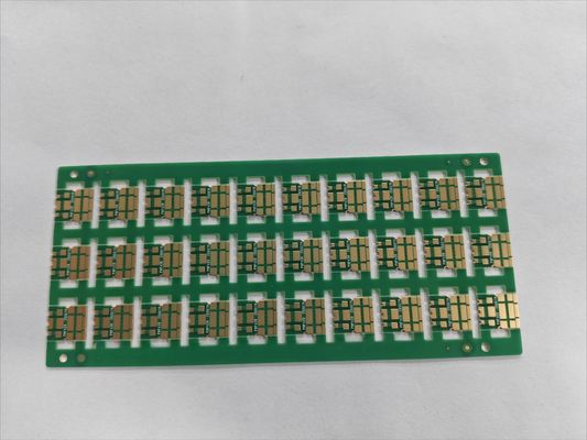
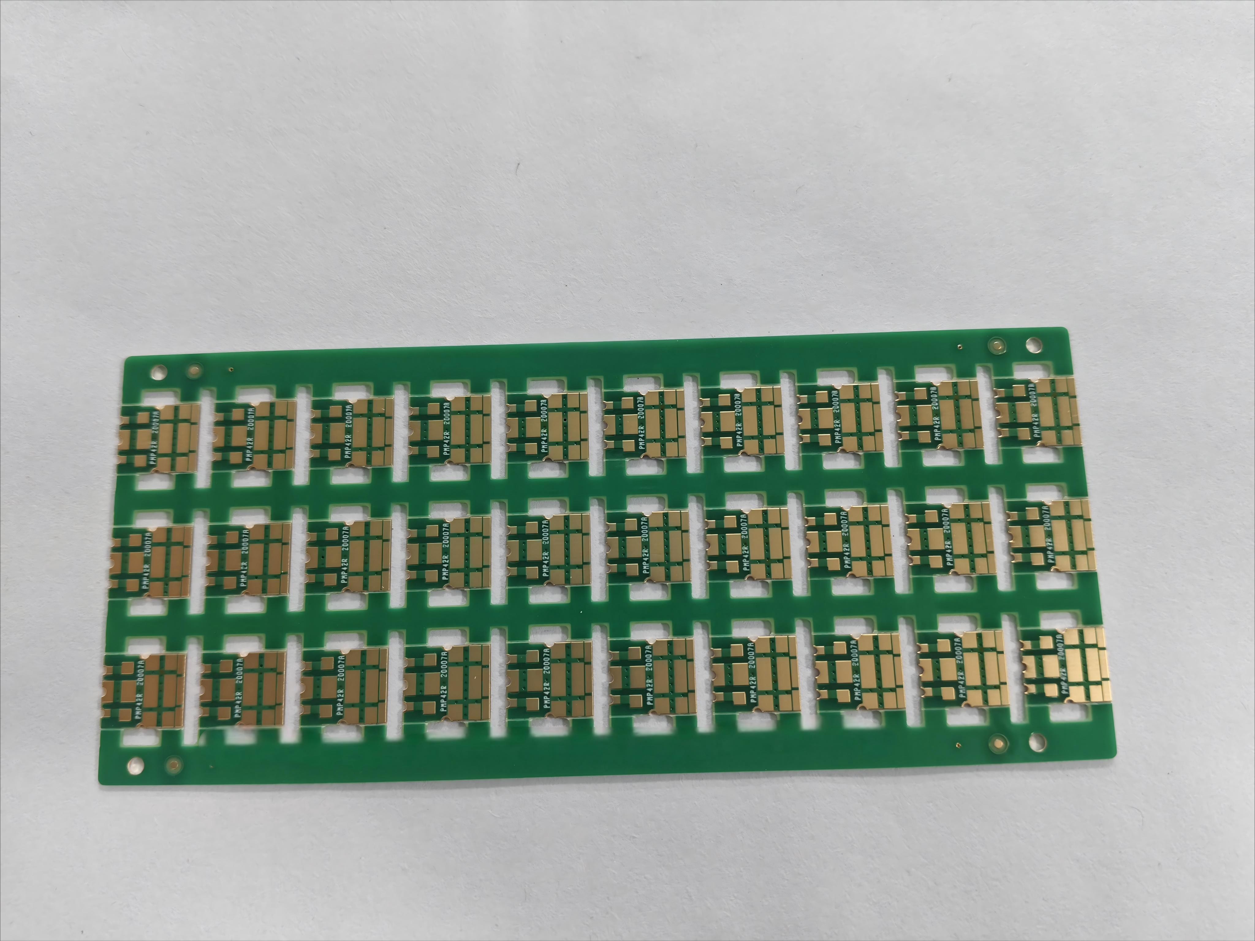
8-Layer FR4 HF Encoder Precision PCB Thickness 3.0mm

| Place of Origin | China Shenzhen |
|---|---|
| Brand Name | JIETENG |
| Certification | UL ROHS TS16949 |
| Model Number | Encoder Precision Pcb |

Contact me for free samples and coupons.
Whatsapp:0086 18588475571
Wechat: 0086 18588475571
Skype: sales10@aixton.com
If you have any concern, we provide 24-hour online help.
xProduct Details
| Silkscreen Color | White | Solder Mask Color | Green |
|---|---|---|---|
| Test Method | Flying Probe Test | PCB Layer | 8-Layer |
| Surface Finish | HASL, ENIG | Product Name | Product Name: Encoder Precision PCB Surface Treatment: HASL Minimum Aperture: 0.2mm PCB Material: FR4 HF Material PCB Layers: 8 Layers Silk Screen Color: White This Product Is A Printed Circuit Board Assembly, Providing Prototype PCB Assembly Manufacturing |
| PCB Material | FR4 HF Material | PCB Thickness | 3.0mm |
| Highlight | HF Encoder Precision PCB,3.0mm FR4 Precision PCB,8-Layer FR4 PCB |
||
Product Description
Features:
Product Name: Encoder Precision PCB
Surface Treatment: HASL
Minimum Aperture: 0.2mm
PCB Material: FR4 HF Material
PCB Layers: 8 Layers
Silk Screen Color: White
This product is a printed circuit board assembly, providing prototype PCB assembly manufacturing services. It features HASL surface treatment, minimum aperture of 0.2mm, and 8-layer PCB made of FR4 HF material. The silk screen color is white.
Technical Parameters:
| PCB Material | FR4 HF Material |
| PCB Layer | 8-Layer |
| Min Hole Size | 0.2mm |
| Test Method | Flying Probe Test |
| Copper Weight | 1oz |
| Solder Mask Color | Green |
| Silkscreen Color | White |
| PCB Thickness | 3.0mm |
| Surface Finish | HASL |
| Product Name | Encoder Precision Pcb |
Applications:
The encoder precision PCB is ideal for a variety of applications, including industrial automation, robotics, and medical devices.
The JIETENG prototype PCB assembly has a copper weight of 1 ounce, and the product uses a flying probe test method to ensure that it meets the highest quality control and reliability standards.
It is suitable for a variety of scenarios, including prototyping, product development, and small-scale production runs. This product is ideal for applications that require high precision and accuracy, such as telecommunications, computer hardware, and consumer electronics.
FAQ:
Q: How long is the lead time for JIETENG Prototype PCB Assembly?
A: The lead time for JIETENG Prototype PCB Assembly is usually 10-13 working days, depending on the complexity of the design and the order quantity.
Q: Does JIETENG Prototype PCB Assembly offer any customization options?
A: Yes, JIETENG Prototype PCB Assembly provides Gerber files and technical requirements. Such as PCB material, thickness, copper surface, mask and silk screen color, etc.
Q: Where is JIETENG Prototype PCB Assembly manufactured?
A: JIETENG Prototype PCB Assembly is manufactured in Shenzhen, China.
Q. What file formats are accepted for PCB production?
A: Gerber files: CAM350 PCB files: Protel 99SE, PADS, CAD, Altium Designer.
Q. Are my files safe?
A: Your files are completely safe. We protect our customers' intellectual property rights throughout the process. All files of customers will never be shared with any third party.
![]()
Recommended Products