

All Products
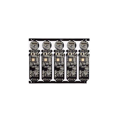
4oz Copper Green Solder Mask Multi Layer PCB Manufacturing with 0.1mm Min. Line Spacing

| Place of Origin | China |
|---|---|
| Brand Name | JIETENG |
| Model Number | Multilayer PCB Fabrication |
| Minimum Order Quantity | Negotiable |
| Price | Negotiable |
| Packaging Details | Blank carton, vacuum packed |
| Delivery Time | 5-8 working day |
| Payment Terms | Negotiable |
| Supply Ability | 360000 square meters / year |

Contact me for free samples and coupons.
Whatsapp:0086 18588475571
Wechat: 0086 18588475571
Skype: sales10@aixton.com
If you have any concern, we provide 24-hour online help.
xProduct Details
| Surface Finish | HASL, ENIG, OSP, Immersion Silver, Immersion Tin, Etc. | Solder Mask Color | Green, Blue, White, Black, Red, Etc. |
|---|---|---|---|
| Copper Thickness | 1-4oz | Min. Hole Size | 0.2mm |
| Board Thickness | 0.2mm-6.0mm | Material | FR4, High TG FR4, Halogen Free, Rogers, Etc. |
| Min. Line Spacing | 0.1mm | Impedance Control | Yes |
| Base Materil | FR4 | Surface Finishing | Immersion Gold |
| Conductor Space | 4 Mil | Testing | Flying Probe Test, E-test, X-ray Inspection, Etc. |
| Standard | IPC Standard | Category | Multilayer PCB |
| Prodcut Type | OEM&ODM | Blades Type | One Circcle Blade And One Linear Blade |
| Board Thick | 2.0 Mm | Color | Green,Blue,Black,Red,Yellow Etc. |
| Type | Electronic Board | Pcb Standard | IPC-A-610 D |
| Highlight | 4oz Copper Multi Layer PCB,Green Solder Mask Multi Layer PCB |
||
Product Description
Product Description:
We offer a minimum Line Spacing and Line Width of 0.1mm, ensuring that your PCBs are precise and efficient. Our Multilayer PCB Fabrication service also offers a range of Solder Mask Colors, including Green, Blue, White, Black, Red, and more. This allows you to customize your PCBs to match your specific needs and preferences.
Our Silkscreen Colors include White, Black, Yellow, and more. This allows you to add important information to your PCBs, such as component labels or assembly instructions. With our Multilayer PCB Manufacturing service, you can be sure that your PCBs will be of the highest quality and meet your exact requirements.
Features:
- Product Name: Multilayer PCB Fabrication
- Min. Line Spacing: 0.1mm
- Impedance Control: Yes
- Layer Count: 2-20
- Material: FR4, High TG FR4, Halogen Free, Rogers, Etc.
- Solder Mask Color: Green, Blue, White, Black, Red, Etc.
Our Multilayer PCB Fabrication service offers:
- Multi-Layer Printed Circuit Board Production
- Multi-Layer PCB Manufacturing
- Multi-Level Printed Circuit Board Fabrication
Applications:
The PCB circuit board has a minimum line width and spacing of 0.1mm, making it ideal for Multi-Level Printed Circuit Board Fabrication. The copper thickness ranges from 1-4oz, making it suitable for different types of electronic devices. The material used in the production of this product includes FR4, High TG FR4, Halogen Free, Rogers, and other high-quality materials that ensure durability and reliability.
The PCB circuit board is an essential component in electronic devices. It is used in various applications, including telecommunications, automotive, medical, and consumer electronics. This product can be used in Multi-Layer PCB Component Assembly, which is a process used in the manufacturing of complex electronic devices.
The JIETENG PCB circuit board is designed to meet the needs of different industries, making it a versatile and reliable product. It can be used in the production of smartphones, laptops, tablets, and other electronic devices. The product is manufactured using the latest technology and is subjected to strict quality control measures to ensure that it meets industry standards.
Overall, the JIETENG PCB circuit board is a high-quality product that is suitable for Multi-Layer Printed Circuit Board Production, Multi-Level Printed Circuit Board Fabrication, and Multi-Layer PCB Component Assembly. The product is durable, reliable, and versatile, making it an ideal choice for various applications and scenarios.
Customization:
- Min. line width: 0.1mm
- Silkscreen color options: white, black, yellow, etc.
- Impedance control: yes
- Board thickness: 0.2-3.2mm
- Min. hole size: 0.2mm
Trust us to deliver reliable and efficient multi-level printed wiring board creation services for your next project. Contact us today to learn more about our customization options.
Support and Services:
The Multilayer PCB Fabrication product offers technical support and services to ensure the highest quality of PCBs. Our team of experts can assist with design optimization, material selection, and production processes to optimize performance and reduce costs.
We offer a range of services including PCB layout design, prototyping, and full-scale production. Our state-of-the-art facilities and advanced equipment ensure that we can meet the most demanding specifications with accuracy and precision.
Our technical support team is available to answer any questions and provide guidance throughout the product lifecycle. We also offer testing and verification services to ensure that the final product meets all quality and regulatory standards.
With our commitment to quality and customer satisfaction, you can trust us to deliver reliable and high-performance PCBs for your applications.
Packing and Shipping:
Product Packaging:
- The Multilayer PCB Fabrication product will be securely packaged in anti-static bags.
- The anti-static bags will be placed in a sturdy cardboard box.
- The cardboard box will be sealed with packing tape.
Product Shipping:
- The Multilayer PCB Fabrication product will be shipped via a trusted courier service.
- The shipping cost will be calculated based on the customer's location and the weight of the package.
- Customers will be provided with a tracking number to track their package during transit.
- The estimated delivery time will be provided to the customer based on their location and the courier service used.
Recommended Products