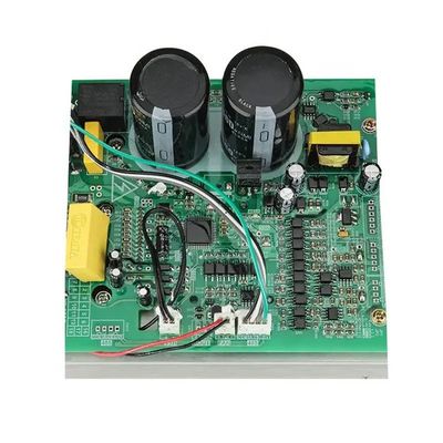
Impedance Control Multilayer PCB Fabrication With Green Red Blue Solder Mask 3oz Copper Rogers

Contact me for free samples and coupons.
Whatsapp:0086 18588475571
Wechat: 0086 18588475571
Skype: sales10@aixton.com
If you have any concern, we provide 24-hour online help.
x| Impedance Control | Yes | Layer Count | 2-20 |
|---|---|---|---|
| Solder Mask Color | Blue.green Etc | Min. Line Spacing | 0.1mm |
| Min. Hole Size | 0.2mm | Surface Finish | HASL, ENIG, OSP, Immersion Silver, Immersion Tin, Etc. |
| Copper Thickness | 3OZ | Silkscreen Color | White, Black, Yellow, Etc. |
| Testing Service | AOI, E-test, Function Test, Etc. | Application | Electronic Manufacturing Services |
| Components | Surface Mount Devices | Solder Mask | White Black Yellow Green Red |
| Solder Paste Printing Accuracy | ±0.05mm | Pcb Size | 100mm*100mm |
| Assembly Process | Pick And Place | Components Pitch | 0.5mm |
| Mounting Style | Top Mount | Fineshed Board Thickness | 0.3mm-3.5mm |
| Pcb Standard | IPC-II Standard | Certifications | ISO 9001:2015, RoHS, UL |
| Highlight | Impedance Control Multilayer PCB,Red Blue Solder Mask Multilayer PCB,3oz Copper Multilayer PCB |
||
Product Description:
We offer a wide range of Solder Mask Color options like Green, Blue, White, Black, Red, etc. Choose the color that suits your design and branding requirements.
Our Multi-Layer PCB Manufacturing service offers different Material options like FR4, High TG FR4, Halogen-Free, Rogers, etc. Choose the material that best meets your specific application requirements.
Surface Finish is crucial in PCBs, and we have you covered. Our Multi-Layer PCB Manufacturing service offers different Surface Finish options like HASL, ENIG, OSP, Immersion Silver, Immersion Tin, etc. Choose the Surface Finish that suits your design and application requirements.
Our Multi-Layer PCB Manufacturing service offers Board Thickness options ranging from 0.2-3.2mm. Choose the Board thickness that meets your specific application requirements.
With our Multi-Layer PCB Manufacturing service, you can be sure of high-quality PCBs that meet your requirements. Contact us now, and let's discuss your specific needs.
Features:
- Product Name: Multilayer PCB Fabrication
- Layer Count: 2-20
- Copper Thickness: 1-4oz
- Min. Line Width: 0.1mm
- Board Thickness: 0.2-3.2mm
- Min. Hole Size: 0.2mm
This product is ideal for Multi-Layer PCB Component Assembly, Multi-Level Printed Wiring Board Creation, and Multi-Layer Printed Circuit Board Production.
Applications:
With a range of surface finishes such as HASL, ENIG, OSP, Immersion Silver, Immersion Tin, etc., this product can cater to different needs and preferences. It has a board thickness of 0.2-3.2mm and a copper thickness of 1-4oz, which makes it suitable for different applications. The min. line spacing of 0.1mm enables the product to have high-density circuit designs.
Whether it is for multi-layer PCB component assembly, multi-layer PCB manufacturing, or multi-layer printed circuit board production, JIETENG's PCB circuit board can deliver top-quality results. It can handle complex designs and circuits, and its high precision ensures that the final product meets the required specifications.
The product application occasions and scenarios for JIETENG's PCB circuit board are vast. It can be used in the production of smartphones, computers, tablets, and other electronic devices. The automotive industry can use it in the production of engine control units, dashboard electronics, and safety systems. The medical industry can use it in the production of medical devices, implantable devices, and diagnostic equipment. The telecommunications industry can use it in the production of communication equipment, such as modems, routers, and switches. The aerospace industry can use it in the production of avionics, navigation systems, and communication systems.
Customization:
Support and Services:
The Multilayer PCB Fabrication product technical support and services include:
- Design review and consultation
- Guidance on material selection and PCB stack-up
- Assistance in meeting specific design requirements
- Testing and analysis of PCB prototypes and products
- Troubleshooting and issue resolution
- Documentation and technical resources
- Training and education on PCB design and fabrication
Packing and Shipping:
Product Packaging:
- All multilayer PCBs will be packed in anti-static bags to prevent damage from static electricity.
- The anti-static bags will then be placed in protective foam or bubble wrap to further safeguard the PCBs during shipping.
- Finally, the packaged PCBs will be placed in sturdy cardboard boxes with ample padding to prevent any damage during transportation.
Shipping:
- Shipping will be handled by our trusted partners who are experienced in handling delicate electronic components.
- Customers will be provided with tracking information once the product has shipped so they can monitor its progress and estimated delivery date.
- If there are any issues with the product during shipping, we will work with the customer to resolve the matter quickly and efficiently.


