

All Products
Impedance Control 0.1mm Multi Layer PCB Manufacturing With Min. Line Spacing

| Place of Origin | China |
|---|---|
| Brand Name | JIETENG |
| Model Number | PCB circuit board |
| Minimum Order Quantity | Negotiable |
| Price | Negotiable |
| Packaging Details | Blank carton, vacuum packed |
| Delivery Time | 5-8 working day |
| Payment Terms | Negotiable |
| Supply Ability | 360000 square meters / year |

Contact me for free samples and coupons.
Whatsapp:0086 18588475571
Wechat: 0086 18588475571
Skype: sales10@aixton.com
If you have any concern, we provide 24-hour online help.
xProduct Details
| Surface Finish | HASL, ENIG, OSP, Immersion Silver, Immersion Tin, Etc. | Impedance Control | Yes |
|---|---|---|---|
| Min. Line Width | 0.1mm | Min. Line Spacing | 0.1mm |
| Board Thickness | 0.2-3.2mm | Solder Mask Color | Green, Blue, White, Black, Red, Etc. |
| Copper Thickness | 1-4oz | Silkscreen Color | White, Black, Yellow, Etc. |
| Highlight | 0.1mm Multi Layer PCB Manufacturing,Impedance Control Multi Layer PCB Manufacturing |
||
Product Description
Product Description:
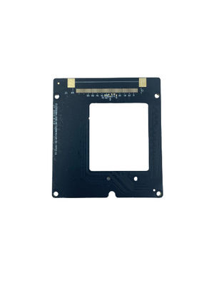
Impedance Control Yes With Min. Line Spacing 0.1mm Multi - Layer PCB Manufacturing
Multi-Layer PCB Manufacturing is an advanced method of producing printed circuit boards (PCBs) for use in a variety of electronic applications. It involves the fabrication and assembly of multiple layers of copper-clad material to create a finished PCB with a greater degree of complexity and functionality than a single-layer board. With our Multi-Layer Printed Circuit Board Production, customers can achieve board thicknesses from 0.2 to 3.2mm, impedance control, and extremely precise min. hole sizes of 0.2mm and min. line spacing of 0.1mm. We also offer a variety of surface finishes including HASL, ENIG, OSP, Immersion Silver, and Immersion Tin. Our cutting-edge Multi-Level Printed Circuit Board Fabrication services are ideal for customers looking to create highly complex and reliable PCBs.
Features:
- Product Name: Multilayer PCB Fabrication
- Surface Finish: HASL, ENIG, OSP, Immersion Silver, Immersion Tin, Etc.
- Min. Line Width: 0.1mm
- Board Thickness: 0.2-3.2mm
- Min. Line Spacing: 0.1mm
- Impedance Control: Yes
- Multi-Level Printed Wiring Board Creation
- Multi-Layer PCB Manufacturing
- Multi-Layer PCB Fabrication
Technical Parameters:
| Parameter | Value |
|---|---|
| Surface Finish | HASL, ENIG, OSP, Immersion Silver, Immersion Tin, etc. |
| Material | FR4, High TG FR4, Halogen Free, Rogers, etc. |
| Layer Count | 2-20 |
| Copper Thickness | 1-4oz |
| Min. Hole Size | 0.2mm |
| Solder Mask Color | Green, Blue, White, Black, Red, etc. |
| Silkscreen Color | White, Black, Yellow, etc. |
| Impedance Control | Yes |
| Min. Line Spacing | 0.1mm |
| Min. Line Width | 0.1mm |
Applications:
JIETENG's Multi-Layer PCB Fabrication is a great choice for any application that requires high precision and accuracy. It is suitable for a wide range of applications, such as manufacturing of printed circuit boards, component assembly, and multi-level printed wiring board creation. Our Multi-Layer PCB Fabrication is made of high-quality materials such as FR4, high TG FR4, halogen free, Rogers, and so on. It provides superior durability and performance with its board thickness ranging from 0.2 to 3.2mm. The silkscreen color of the PCB is available in white, black, yellow, etc. and the min. hole size is 0.2mm. Moreover, the layer count of this product can be customized from 2 to 20.
Customization:
Customized Multi-Layer PCB Fabrication Services from JIETENG
JIETENG provides customized multi-layer PCB fabrication services, which can be used for multi-level printed circuit board fabrication and multi-layer printed circuit board production.
Our multi-layer PCB fabrication services are available for a wide range of brand names and model numbers. Our PCB circuit boards are manufactured using high-quality materials and the latest technologies. We can also provide customized solutions to meet your specific requirements.
Our multi-layer PCB fabrication services are available with a minimum line width of 0.1mm and copper thickness of 1-4oz. We also offer a variety of silkscreen colors including white, black, yellow, etc. You can also choose from a range of layer counts from 2-20. Our surface finish options include HASL, ENIG, OSP, Immersion Silver, Immersion Tin, etc.
Support and Services:
Multilayer PCB Fabrication Technical Support and Service
We offer comprehensive technical support and service for our Multilayer PCB Fabrication products. Our experienced and knowledgeable engineers are available to answer any questions you may have about our products and processes.
We offer a variety of technical services, including:
- Design assistance for custom applications
- Advice on materials selection and fabrication processes
- Troubleshooting of existing designs
- On-site training for use of our products
- Guidance on regulatory and safety issues
Our technical support team can be reached by phone, email, or live chat. We are committed to providing the best possible service and support for our customers.
Packing and Shipping:
Packaging and Shipping for Multilayer PCB Fabrication:
We will ship the Multilayer PCB Fabrication in protective packaging to ensure it arrives to your destination safely. All packages will be inspected for damage before shipping and securely sealed to prevent any further damage during transit.
We provide a variety of shipping options to best suit your needs, including air freight, sea freight, express delivery, and local pickup. Our shipping charges are calculated based on the weight of the product, the destination, and the shipping method you choose.
FAQ:
- Q: What is the brand name of the product?
- A: The brand name of the product is JIETENG.
- Q: What is the model number of the product?
- A: The model number of the product is PCB circuit board.
- Q: Where is the product made?
- A: The product is made in China.
- Q: What is the multilayer PCB fabrication?
- A: Multilayer PCB fabrication is the process of producing a printed circuit board with multiple layers.
- Q: What components are used in the fabrication process?
- A: The components used in the fabrication process may include copper foil, prepreg, laminate, solder mask and silkscreen.
Recommended Products