

All Products
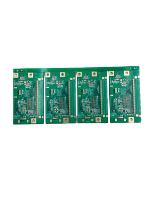
Bubble Bag Packaging High Frequency PCBs Board Thickness 0.2-3.2mm With FR4

| Place of Origin | China |
|---|---|
| Brand Name | JIETENG |
| Model Number | PCB circuit board |
| Minimum Order Quantity | Negotiable |
| Price | Negotiable |
| Packaging Details | Blank carton, vacuum packed |
| Delivery Time | 5-8 working day |
| Payment Terms | Negotiable |
| Supply Ability | 360000 square meters / year |

Contact me for free samples and coupons.
Whatsapp:0086 18588475571
Wechat: 0086 18588475571
Skype: sales10@aixton.com
If you have any concern, we provide 24-hour online help.
xProduct Details
| Silk Screen Color | White, Black, Yellow, Etc. | Min Hole Size | 0.2mm |
|---|---|---|---|
| Packaging | Vacuum Packing, Bubble Bag, Carton Box, Etc. | Material | FR4 |
| Copper Thickness | 1-4oz | Board Thickness | 0.2-3.2mm |
| Min Trace Width/Space | 3/3mil | Impedance Control | ±10% |
| Highlight | High Frequency PCBs Board,3.2mm High Frequency PCBs |
||
Product Description
Product Description:
High-frequency circuit boards, also known as high-speed printed boards or high-performance circuit boards, are printed circuit boards (PCBs) designed to meet the need for high-speed, high-frequency electronic devices. These boards are manufactured with a range of features, including silk screen colors such as white, black, yellow and others; board thickness ranging from 0.2mm to 3.2mm; impedance control of ±10%; copper thickness of 1-4oz; and a minimum hole size of 0.2mm. High-frequency circuit boards are designed to meet the rigorous demands of high-speed, high-frequency applications.
Features:
- High-Frequency Printed Circuit Boards: Vacuum Packing, Bubble Bag, Carton Box, Etc., Min Trace Width/Space: 3/3mil, Impedance Control: ±10%, Layer: 2-10, Solder Mask Color: Green, Blue, White, Black, Etc.
- High-Speed Circuit Boards: Vacuum Packing, Bubble Bag, Carton Box, Etc., Min Trace Width/Space: 3/3mil, Impedance Control: ±10%, Layer: 2-10, Solder Mask Color: Green, Blue, White, Black, Etc.
- High-Frequency Printed Boards: Vacuum Packing, Bubble Bag, Carton Box, Etc., Min Trace Width/Space: 3/3mil, Impedance Control: ±10%, Layer: 2-10, Solder Mask Color: Green, Blue, White, Black, Etc.
Technical Parameters:
| Parameter | Value |
|---|---|
| Product | High-Speed Printed Circuit Boards, High-Frequency Printed Boards, High-Speed Circuit Boards |
| Layer | 2-10 |
| Packaging | Vacuum Packing, Bubble Bag, Carton Box, Etc. |
| Solder Mask Color | Green, Blue, White, Black, Etc. |
| Impedance Control | ±10% |
| Copper Thickness | 1-4oz |
| Min Trace Width/Space | 3/3mil |
| Min Hole Size | 0.2mm |
| Surface Finish | HASL, ENIG, OSP, Etc. |
| Silk Screen Color | White, Black, Yellow, Etc. |
| Material | FR4 |
Applications:
High-Performance Printed Circuit Boards from JIETENG are widely used in a variety of applications and industries. These boards are designed to provide reliable, high-speed performance and superior electrical properties. Their features include a variety of solder mask colors, such as green, blue, white, black, and more; board thicknesses from 0.2 to 3.2mm; and an impressive minimum trace width/space of 3/3 mil. The boards are also made of high-quality FR4 material and come with vacuum packing, bubble bag, and carton box packaging to ensure safe transportation and delivery. With its superior electrical properties and high-speed performance, JIETENG’s High-Performance Printed Circuit Boards provide a reliable solution for many different applications.
Customization:
High-Frequency Printed Boards: Customized for Your Needs
JIETENG offers high frequency PCBs that are manufactured to your exact specifications. Our high-frequency circuit boards are capable of withstanding extreme environmental conditions and provide impedance control of ±10%.
Our boards are available in a variety of thicknesses, ranging from 0.2mm to 3.2mm. We offer a wide range of solder mask colors, including green, blue, white, and black. All of our boards are made of FR4 material and are available with a variety of surface finishes, including HASL, ENIG, and OSP.
If you're looking for high-quality, high-frequency printed boards, then look no further than JIETENG!
Support and Services:
High Frequency PCBs Technical Support and Service
- Provide technical assistance to customers in the selection of materials and design of high-frequency PCBs.
- Provide technical advice and solutions to customers to improve the performance of high-frequency PCBs.
- Assist customers in troubleshooting and repairing high-frequency PCBs.
- Provide on-site technical support for high-frequency PCBs.
- Provide customer feedback on high-frequency PCBs.
- Provide training and guidance for customers on high-frequency PCBs.
- Provide online technical support and services for customers on high-frequency PCBs.
Packing and Shipping:
Packaging and Shipping for High Frequency PCBs
High Frequency PCBs must be packaged and shipped with special care to ensure that the boards arrive undamaged. Here are the steps for packaging and shipping High Frequency PCBs:
- Carefully wrap the PCBs in bubble wrap or other protective material. This prevents damage from static electricity.
- Place the bubble-wrapped PCBs inside a static-shielding bag.
- Put the static-shielding bag inside an antistatic shipping box.
- Place the antistatic shipping box in another cardboard shipping box.
- Pack the cardboard shipping box with foam peanuts or other cushioning material.
- Seal the cardboard shipping box and label it as containing high frequency electronic components.
- Ship the package using a reputable shipping service.
FAQ:
- Q:What is the brand name of the High Frequency PCBs?
- A:The brand name of the High Frequency PCBs is JIETENG.
- Q:What is the model number of the High Frequency PCBs?
- A:The model number of the High Frequency PCBs is PCB circuit board.
- Q:Where is the High Frequency PCBs made?
- A:The High Frequency PCBs are made in China.
- Q:What material is used to make High Frequency PCBs?
- A:High Frequency PCBs are made of high-quality FR4 material and copper foil.
- Q:What is the application of High Frequency PCBs?
- A:High Frequency PCBs are mainly used in high frequency wireless communication products, such as mobile phones, base stations, satellite communication systems, etc.
Recommended Products