

All Products
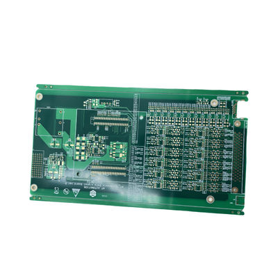
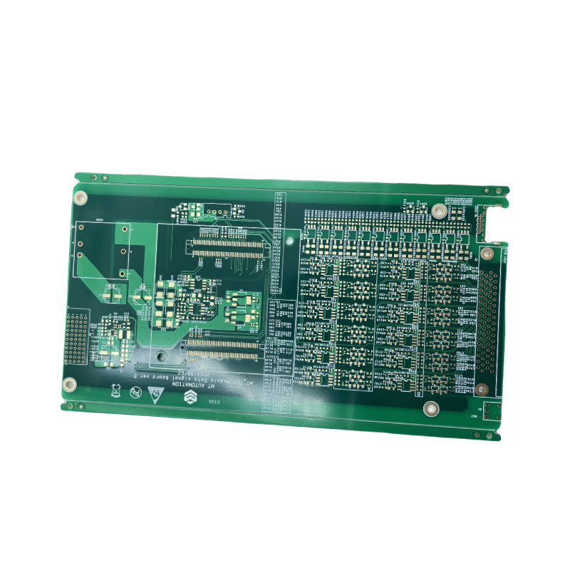
Green Solder Mask Multilayer Pcb Fabrication Immersion Tin

| Place of Origin | China |
|---|---|
| Brand Name | JIETENG |
| Certification | ISO/TS16949/RoHS/TS16949 |
| Model Number | PCB circuit board |
| Minimum Order Quantity | Negotiable |
| Price | Negotiable |
| Packaging Details | Blank carton, vacuum packed |
| Delivery Time | 5-8 working day |
| Payment Terms | Negotiable |
| Supply Ability | 360000 square meters / year |

Contact me for free samples and coupons.
Whatsapp:0086 18588475571
Wechat: 0086 18588475571
Skype: sales10@aixton.com
If you have any concern, we provide 24-hour online help.
xProduct Details
| Solder Mask Color | Green, Blue, White, Black, Red, Etc. | Silkscreen Color | White, Black, Yellow, Etc. |
|---|---|---|---|
| Material | FR4, High TG FR4, Halogen Free, Rogers, Etc. | Copper Thickness | 1-4oz |
| Surface Finish | HASL, ENIG, OSP, Immersion Silver, Immersion Tin, Etc. | Min. Line Width | 0.1mm |
| Board Thickness | 0.2-3.2mm | Layer Count | 2-20 |
| Highlight | green solder mask multilayer pcb fabrication,immersion tin multilayer pcb fabrication,green solder mask rogers pcb fabrication |
||
Product Description
Product Description:
Multi-Layer PCB Fabrication is a comprehensive service that provides precision manufacturing of multi-layer PCBs with high quality and accuracy. The service covers a wide array of materials, including FR4, high TG FR4, halogen free, Rogers, and other specialized materials. The minimum hole size that can be achieved is 0.2mm while the copper thickness can range from 1 to 4 ounces. Impedance control is also available to ensure that the final product meets exacting standards. In addition, the service also offers a wide range of silkscreen colors, including white, black, yellow, and other customized colors to meet customer needs. The Multi-Layer PCB Fabrication service also provides component assembly and other related services to ensure that the final product is delivered in a timely and efficient manner.
Features:
- Product Name: Multilayer PCB Fabrication
- Board Thickness: 0.2 - 3.2mm
- Layer Count: 2 - 20
- Impedance Control: Yes
- Materials: FR4, High TG FR4, Halogen Free, Rogers, Etc.
- Surface Finish: HASL, ENIG, OSP, Immersion Silver, Immersion Tin, Etc.
- Multi-Level Printed Circuit Board Fabrication: Yes
- Multi-Layer PCB Manufacturing: Yes
- Multi-Layer PCB Component Assembly: Yes
Technical Parameters:
| Property | Description |
|---|---|
| Board Thickness | 0.2-3.2mm |
| Min. Line Width | 0.1mm |
| Min. Line Spacing | 0.1mm |
| Min. Hole Size | 0.2mm |
| Material | FR4, High TG FR4, Halogen Free, Rogers, Etc. |
| Copper Thickness | 1-4oz |
| Solder Mask Color | Green, Blue, White, Black, Red, Etc. |
| Layer Count | 2-20 |
| Impedance Control | Yes |
| Silkscreen Color | White, Black, Yellow, Etc. |
| Multi-Layer PCB Manufacturing | Yes |
| Multi-Layer PCB Component Assembly | Yes |
| Multi-Level Printed Wiring Board Creation | Yes |
Applications:
JIETENG, with its model number PCB circuit board, is a reputable Chinese manufacturer of multi-layer PCB components, assemblies and printed circuit boards. It is renowned for its advanced impedance control technology and high precision manufacturing capabilities. The multi-layer PCBs are available in layer counts ranging from 2 to 20. The minimum line spacing of 0.1mm ensures that the PCBs can pack in more components and perform complex functions. The silkscreen color is available in white, black, yellow and other colors, and the min. hole size is 0.2mm.
JIETENG’s multi-layer printed circuit board production involves intricate processes such as lamination, etching, drilling, plating, and soldering. Its advanced multi-layer PCB component assembly and manufacturing technology ensures superior product quality, reliability and performance. With its superior assembly and manufacturing capabilities, JIETENG is the ideal partner for customers who require high-quality multi-layer PCB components and assemblies.
Customization:
JIETENG Multi-Level Printed Circuit Board Fabrication Services
JIETENG is a leading provider of Multi-Level Printed Wiring Board Creation and Multi-Level Printed Circuit Board Fabrication services in China. Our Multi-Level Printed Circuit Board Fabrication services provide superior quality and reliability.
We use the latest technologies to ensure that your Multi-Level Printed Circuit Board Fabrication is of the highest quality. Our Multi-Level Printed Circuit Board Fabrication services can meet the most demanding requirements, including:
- Min. Hole Size: 0.2mm
- Surface Finish: HASL, ENIG, OSP, Immersion Silver, Immersion Tin, Etc.
- Min. Line Spacing: 0.1mm
- Material: FR4, High TG FR4, Halogen Free, Rogers, Etc.
- Silkscreen Color: White, Black, Yellow, Etc.
Our Multi-Level Printed Circuit Board Fabrication services are used by leading companies in the industry. Contact us today to learn more about our Multi-Level Printed Circuit Board Fabrication services and how we can help you create the best Multi-Level Printed Circuit Board for your specific needs.
Support and Services:
Multilayer PCB Fabrication Technical Support and Service
Multilayer printed circuit board (PCB) fabrication requires a combination of specialized skills and processes. Our experienced engineers provide a variety of technical support and services to ensure the highest quality parts and materials for the best performance of your PCBs.
Our technical support and services include:
- Design and layout consultation
- Materials selection and sourcing
- Fabrication process optimization
- Testing and troubleshooting
- Assembly and integration
We understand that every application is unique, so we strive to offer tailored solutions to meet your specific needs. Our team of experts is ready to help you get the best out of your multilayer PCB fabrication project.
Packing and Shipping:
Packaging and Shipping for Multilayer PCB Fabrication
Packaging and shipping are important aspects of the Multilayer PCB Fabrication process. To ensure that the boards are delivered safely and securely, they are carefully packed and shipped to their destination. This includes:
- Using anti-static bags to protect the PCBs from static electricity.
- Using bubble wrap to cushion the PCBs against shocks during transport.
- Using sturdy boxes to protect the PCBs from drops, vibrations, and other environmental factors.
- Using foam or foam inserts to help keep the PCBs in place during transit.
- Using proper labeling to ensure that the package is delivered to the correct destination.
Once the package is ready for shipping, it is sent to the designated address via a reliable courier service. The package is tracked throughout its transit to ensure that it reaches its destination safely and on time.
FAQ:
- Q1: What is Multilayer PCB Fabrication?
- A1: Multilayer PCB Fabrication is the process of making a circuit board with multiple layers using JIETENG's PCB circuit board which is made in China.
- Q2: What are the benefits of using Multilayer PCB Fabrication?
- A2: Multilayer PCB Fabrication offers higher density, improved heat dissipation, better signal integrity, increased design flexibility, and improved reliability.
- Q3: How many layers can a Multilayer PCB Fabrication have?
- A3: The number of layers depends on the application and complexity of the design, but typically ranges from 2 to 16 layers.
- Q4: What materials are used in Multilayer PCB Fabrication?
- A4: Commonly used materials for Multilayer PCB Fabrication include copper, epoxy, glass woven fabric, and polyimide.
- Q5: What types of products can be manufactured with Multilayer PCB Fabrication?
- A5: Multilayer PCB Fabrication can be used to manufacture a wide range of products, such as cell phones, computers, and medical devices.
Recommended Products