


All Products
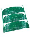
Customized Multilayer PCB Circuit Board Design For Electronics Device

| Place of Origin | Guangdong, China |
|---|---|
| Brand Name | JIETENG |
| Certification | ISO/TS16949/RoHS/TS16949 |
| Model Number | PCB |
| Minimum Order Quantity | Negotiable |
| Price | Negotiable |
| Packaging Details | Inner vacuum packing, outer standard carton |
| Delivery Time | 3-10 days for delivery |
| Payment Terms | Negotiable |
| Supply Ability | 150000 Square Meter/Square Meters per Year |

Contact me for free samples and coupons.
Whatsapp:0086 18588475571
Wechat: 0086 18588475571
Skype: sales10@aixton.com
If you have any concern, we provide 24-hour online help.
xProduct Details
| Highlight | Customized Multilayer PCB Circuit Board,Electronics Device Multilayer PCB Circuit Board,Electronics Device Multilayer PCB Design |
||
|---|---|---|---|
Product Description
Factory Customized Multilayer PCB Circuit Board Product
Essential details
| tem | ||
| Type of Alum board | single board, Insulation board, double sided board | |
| Finish Board Thickness | 0.4mm----- 3.0mm | |
| Copper Thickness | 1 OZ--6 OZ | |
| Min.Trace Width & Line Spacing | 0.15mm | |
| Biggest size | 120cm*60cm | |
| Type for surface treatment | OSP.HASL, Immersion Gold ,Immersion Tin (lead free) | |
| OSP | 0.20-0.40um | |
| Thickness of Ni | 2.50-3.50um | |
| Thickness of Au | 0.05-0.10um | |
| Thickness of tin | 5-20um | |
| Thickness of immersion silver | 0.15-0.40um | |
| Thermal conductivity | 1.0W -----3.0W | |
| Dielectric Thickness | 50um-150um | |
| Thermal resistance | 0.05℃/W -1.7℃/W | |
| Minimum completed hole dimension | ±0.10mm | |
| Tolerance for Hole Diameter | ±0.075mm | |
| Minimum Drilling Hole Diameter | φ0.8mm | |
| Mask between pins | 0.15mm-0.35mm | |
| Minimum spacing between Pad and Pad | 0.18mm-0.35mm | |
| Outline tolerance | ±0.10mm | |
| Minimum thickness for V-cut | 0.25mm | |
| Outside copper thickness | 18-105um | |
![]()
Recommended Products