All Products
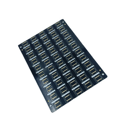
2-32 Layers PCB Circuit Board For Facial Acne Physiotherapy Instrument
| Place of Origin | Guangdong, China |
|---|---|
| Brand Name | JIETENG |
| Certification | ISO/TS16949/RoHS/TS16949 |
| Model Number | PCBA |
| Minimum Order Quantity | Negotiable |
| Price | Negotiable |
| Packaging Details | Inner vacuum packing, outer standard carton |
| Delivery Time | 5-8 days for delivery |
| Payment Terms | Negotiable |
| Supply Ability | 150000 Square Meter/Square Meters per Year |

Contact me for free samples and coupons.
Whatsapp:0086 18588475571
Wechat: 0086 18588475571
Skype: sales10@aixton.com
If you have any concern, we provide 24-hour online help.
xProduct Details
| Pcb Size | 330x50-250mm | Feeder Capacity | 42/84 Slots (option) |
|---|---|---|---|
| Speed | 26000chips/h | Material | STEEL |
| Lead Time | 1-3 Days After Payment | Number Of Layers | 2 - 32 Layers |
| Highlight | 6mm PCB Circuit Board,HASL PCB Circuit Board,32 Layers SMT Assembly Service |
||
Product Description
Development of PCB circuit board for facial acne physiotherapy instrument
|
Products Description
|
||
|
SMT Lines
|
10 Lines
|
|
|
Capacity
|
8 Million Placements Per Day
|
|
|
Max Board Size
|
680*550mm Smallest:0.25"*0.25"
|
|
|
Min Components size
|
0201-54 sq.mm (0.084 sq.inch),Long Connector,CSP,BGA,QFP
|
|
|
Speed
|
0.15sec/chip, 0.7sec/QFP
|
|
|
wave-Solder
|
Max.PCB Width:450mm
|
|
|
Min.PCB Width:unlimited
|
|
|
|
Components Height:Top 120mm/Bot 15mm
|
|
|
|
Sweat-Solder
|
Metal Types:Part,Whole,Inlay,Side-step
|
|
|
Metal Material:Copper,Aluminum
|
|
|
|
Surface Finish:Plating Au,Plating Silver,Plating Sn
|
|
|
|
Air Bladder Rate:less than 20%
|
|
|
|
Press-fit
|
Press Range:0-50KN
|
|
|
Max.PCB Size:800*600mm
|
|
|
|
Assembly Types
|
SMT and Thru-hole
|
|
|
Solder Type
|
Water Soluble Solder Paste,Leaded and Lead-Free
|
|
|
File Formats
|
Bill of Materials ,Gerber Files,Pick-N-Place Files(XYRS)
|
|
|
Type of Service
|
Turn-Key,Partial Turn-Kye or Consignment
|
|
|
Component Packaging
|
Cut Tape,Tube Reels Loose,Parts
|
|
|
Turn Time
|
1-15days
|
|
|
Testing
|
XRAY Inspection,AOI Testing ICT,Flying Probe,Burn-in,Function Test
|
|
Recommended Products


