


All Products
Gold Finger Printed Circuit Board Prototype PCB Assembly 6 Layer


| Place of Origin | Guangdong, China |
|---|---|
| Brand Name | JIETENG |
| Certification | ISO/TS16949/RoHS/TS16949 |
| Model Number | PCB |
| Minimum Order Quantity | Negotiable |
| Price | Negotiable |
| Packaging Details | Vacuum package |
| Delivery Time | 5-8 days for delivery |
| Payment Terms | Negotiable |
| Supply Ability | 50000 Square Meter/Square Meters per Month |

Contact me for free samples and coupons.
Whatsapp:0086 18588475571
Wechat: 0086 18588475571
Skype: sales10@aixton.com
If you have any concern, we provide 24-hour online help.
xProduct Details
| Copper Thickness | 1/2OZ | Base Material | FR-4 |
|---|---|---|---|
| Min. Hole Size | 0.2mm | Silkscreen Color | White |
| Layer | 1-32 Layers | ||
| Highlight | Gold Finger Prototype PCB Assembly,Printed Prototype PCB Assembly,Gold Finger printed circuit board prototype |
||
Product Description
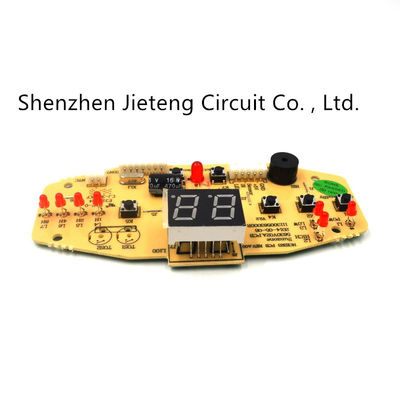
Gold Finger Board 6-layer board game machine motherboard processing
Essential details
![]()
Recommended Products