


All Products
Contact Person :
Sales Manager
Phone Number :
13510910864
Whatsapp :
+8613360524484
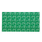
HASL Surface Finish Green PCB 1oz Copper Weight 0.1mm Solder Mask Bridge FR4 Prototype Assembly

| Place of Origin | China |
|---|---|
| Brand Name | JIETENG |
| Model Number | PCB circuit board |
| Minimum Order Quantity | Negotiable |
| Price | Negotiable |
| Packaging Details | Blank carton, vacuum packed |
| Delivery Time | 5-8 working day |
| Payment Terms | Negotiable |
| Supply Ability | 360000 square meters / year |

Contact me for free samples and coupons.
Whatsapp:0086 18588475571
Wechat: 0086 18588475571
Skype: sales10@aixton.com
If you have any concern, we provide 24-hour online help.
xProduct Details
| Surface Finish | HASL | Copper Weight | 1oz |
|---|---|---|---|
| Min Solder Mask Bridge | 0.1mm | Min Hole Size | 0.2mm |
| Solder Mask Color | Green | PCB Thickness | 1.6mm |
| PCB Material | FR4 | PCB Size | 100mm*100mm |
| High Light | 1oz Copper Green PCB,FR4 Prototype Assembly Green PCB,HASL Surface Finish Green PCB |
||
Product Description
Product Description:
The Prototype PCB Assembly product is a cutting-edge solution designed for a wide range of applications that require quick turnaround and high precision. This product is an ideal choice for engineers, designers, and manufacturers who require a robust, reliable, and efficient Printed Board Assembly (PBA). With its advanced features and specifications, the Prototype PCB Assembly stands out in the PCB Assembly Manufacturing industry.
Our Prototype PCB Assembly is crafted with a 1oz copper weight that provides excellent conductivity and durability. The copper layer is crucial for the functionality of the PCB as it helps to distribute power and signal throughout the board effectively. This weight is the standard for most PCBs in the industry, ensuring that the product can handle a variety of electrical loads without compromising on performance or reliability.
One of the most visually noticeable aspects of the Prototype PCB Assembly is the white silkscreen color. The white silkscreen is applied over the solder mask layer and is used for printing labels, symbols, and component outlines, which assist in the assembly and provide a clear and readable reference for technicians and end-users. The contrast between the white silkscreen and the solder mask underneath allows for easy identification of components and test points, which is especially important during the prototyping phase.
When it comes to precision, our Prototype PCB Assembly boasts a minimum annular ring size of 0.1mm. The annular ring is the copper area that surrounds a plated through-hole, and it is critical for creating a strong bond between the component lead and the PCB. A 0.1mm minimum annular ring size ensures that there is sufficient space for reliable solder connections, even on components with the smallest pins, thereby significantly reducing the chances of connection failure.
Our product features a minimum solder mask bridge of 0.1mm as well. The solder mask bridge refers to the minimum distance between two openings in the solder mask. This fine level of detail is essential to prevent solder bridging during component placement and reflow, which can cause electrical shorts. By maintaining a minimum of 0.1mm, the Prototype PCB Assembly ensures that each component is precisely defined and isolated, which is vital for the functionality and longevity of the product.
The Prototype PCB Assembly excels in fine-line technology with a minimum line width and space of 0.1mm/0.1mm. This specification allows for denser routing of traces and more complex circuitry on a smaller board, making it perfect for today's miniaturized electronic requirements. Such fine line detailing is paramount in modern Printed Board Assembly as it allows for increased functionality without the need for larger boards, which is a game-changer in space-constrained applications.
In the realm of PCB Assembly Manufacturing, the Prototype PCB Assembly product is unmatched in its attention to detail and adherence to the highest standards of quality. Each board is meticulously assembled and tested to ensure that it meets the stringent requirements necessary for prototypes and low-volume production runs. The product is not only designed to help you validate your designs quickly but also to transition smoothly into full-scale production once the design is finalized.
To sum up, the Prototype PCB Assembly is an exceptional product that is tailored to meet the needs of modern electronics where precision, reliability, and efficiency are paramount. With features like a 1oz copper weight, white silkscreen color, minimum annular ring, solder mask bridge, and line width/space of 0.1mm, this product sets the standard for high-quality Printed Board Assembly. Whether it's for a startup or a large-scale electronics firm, our Prototype PCB Assembly is the go-to product for all PCB assembly needs.
Features:
- Product Name: Prototype PCB Assembly
- PCB Size: 100mm*100mm
- Test Method: Flying Probe Test
- Min Solder Mask Bridge: 0.1mm
- PCB Layer: 2-Layer
- Min Annular Ring: 0.1mm
- PCB Prototype Fabrication
- Prototype PCB Assembly Fabrication
- Printed Circuit Assembly
Technical Parameters:
| Parameter | Specification |
|---|---|
| Surface Finish | HASL |
| Min Annular Ring | 0.1mm |
| PCB Material | FR4 |
| Test Method | Flying Probe Test |
| Min Line Width/Space | 0.1mm/0.1mm |
| PCB Thickness | 1.6mm |
| Min Hole Size | 0.2mm |
| Copper Weight | 1oz |
| Solder Mask Color | Green |
| Min Solder Mask Bridge | 0.1mm |
Applications:
The JIETENG PCB circuit board is a high-quality prototype PCB assembly product, crafted with precision and expertise in the heart of China. This product is an epitome of technological advancement in the realm of PCB Assembly Manufacturing. With a model number signifying its unique design, this printed board assembly is tailored to meet the stringent requirements of modern electronic applications. The PCB boasts a standard size of 100mm*100mm, making it versatile for a variety of uses.
The 2-Layer configuration of the JIETENG PCB circuit board provides a balanced approach to complexity and cost, suitable for a myriad of scenarios ranging from industrial controls to consumer electronics. The use of a white silkscreen color ensures clear and legible markings for component identification and placement, which is vital during both the assembly process and subsequent maintenance checks. This feature significantly enhances the usability of the printed circuit assembly in complex projects.
With a minimum annular ring of 0.1mm, the PCB guarantees robust connections and longevity, even in applications where it is subject to mechanical stress or thermal cycling. The copper weight of 1oz reflects a commitment to quality and reliability, ensuring that the PCB can handle the required current loads without compromising performance.
The JIETENG PCB circuit board is not just a component; it is the backbone of any electronic product. It is an ideal candidate for prototypes in research and development stages, where modifications are frequent and precision is non-negotiable. Whether it's for a startup working on cutting-edge technology or an educational institution imparting practical knowledge, this PCB stands up to the task.
Moreover, the printed board assembly from JIETENG is an excellent choice for small batch production, where each unit needs to adhere to the highest standards of quality. Companies looking to test their designs in real-world conditions before ramping up production will find this PCB to be an invaluable asset. From medical devices to aerospace components, the robust design and precise manufacturing of this PCB can meet the demands of even the most critical applications.
In summary, the JIETENG PCB circuit board is a versatile, reliable, and precise prototype PCB assembly solution. Its attributes make it suitable for a diverse range of applications and scenarios in the field of PCB Assembly Manufacturing, ensuring that engineers and designers have the right foundation to bring their innovations to life.
Customization:
Brand Name: JIETENG
Model Number: PCB circuit board
Place of Origin: China
PCB Size: 100mm*100mm
Min Line Width/Space: 0.1mm/0.1mm
Min Hole Size: 0.2mm
PCB Layer: 2-Layer
PCB Thickness: 1.6mm
Discover the excellence in Prototype PCB Assembly Fabrication with JIETENG, your partner in high-quality Printed Board Assembly . Our services are rooted in China, focusing on delivering precision-engineered PCB circuit boards with a standard size of 100mm*100mm. We ensure meticulous attention to detail with a minimum line width and space of 0.1mm, complemented by a minimum hole size of 0.2mm, to accommodate the most intricate designs. Our 2-Layer PCBs maintain a standard thickness of 1.6mm, exemplifying our commitment to robust and reliable Printed Circuit Assembly solutions.
Support and Services:
If you require technical support for your Prototype PCB Assembly product, our team is here to help. Our support services are designed to address any questions or issues that may arise during the assembly process. Our experts can provide guidance on component placement, soldering techniques, testing procedures, and more to ensure your prototype meets your specifications and performs as intended.
In addition to troubleshooting assistance, we also offer a range of services to facilitate the development of your prototype. These include design review, material selection advice, and recommendations for design for manufacturability (DFM). Our goal is to help you streamline the assembly process and optimize your PCB for production.
For any technical concerns or service requests, please refer to our comprehensive FAQ section or use our online support resources for quick and easy solutions. We are dedicated to providing you with the quality support and services necessary for the success of your prototype PCB assembly project.
Packing and Shipping:
When packaging the Prototype PCB Assembly product, we ensure the utmost care and precision to protect the delicate components and circuitry. Each PCB is first placed in an anti-static bag to prevent electrostatic discharge, which could damage the electronic parts. The bag is then cushioned with foam or bubble wrap and placed in a sturdy, corrugated cardboard box that provides ample protection against impacts and vibrations during transit. We also include a desiccant pack to absorb any moisture that may have accumulated, ensuring the PCB remains dry.
Before shipping, the box is sealed with high-quality packing tape and clearly labeled with handling instructions to ensure that it is kept in the proper orientation. We also mark the package as fragile to alert carriers to handle it with additional care. The shipping label includes the destination address and a tracking number, allowing both the sender and recipient to monitor the package's progress until delivery. Our goal is to deliver your Prototype PCB Assembly product in perfect condition, ready for immediate use upon arrival.
FAQ:
Q1: What is the brand and model number of the PCB Assembly product?
A1: The brand name of the PCB Assembly product is JIETENG, and the model number is PCB circuit board.
Q2: Where is the JIETENG PCB circuit board manufactured?
A2: The JIETENG PCB circuit board is manufactured in China.
Q3: Can the JIETENG PCB circuit board be customized according to specific requirements?
A3: Yes, the JIETENG PCB circuit board can be customized to meet specific design requirements and specifications.
Q4: What types of PCB assembly services does JIETENG offer?
A4: JIETENG offers a range of PCB assembly services including surface mount technology (SMT), through-hole technology (THT), and mixed-technology assembly. We can accommodate both small batch and large-scale production runs.
Q5: How can I ensure the quality of the JIETENG PCB circuit board?
A5: JIETENG employs rigorous quality control measures throughout the manufacturing process, including inspections and testing to ensure that each PCB circuit board meets the highest quality standards.
Recommended Products