


All Products
Contact Person :
Sales Manager
Phone Number :
13510910864
Whatsapp :
+8613360524484
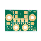
Green Solder Mask Prototype PCB Assembly 2-Layer Flying Probe Test 1.6mm

| Place of Origin | China |
|---|---|
| Brand Name | JIETENG |
| Model Number | PCB circuit board |
| Minimum Order Quantity | Negotiable |
| Price | Negotiable |
| Packaging Details | Blank carton, vacuum packed |
| Delivery Time | 5-8 working day |
| Payment Terms | Negotiable |
| Supply Ability | 360000 square meters / year |

Contact me for free samples and coupons.
Whatsapp:0086 18588475571
Wechat: 0086 18588475571
Skype: sales10@aixton.com
If you have any concern, we provide 24-hour online help.
xProduct Details
| PCB Layer | 2-Layer | Test Method | Flying Probe Test |
|---|---|---|---|
| Min Line Width/Space | 0.1mm/0.1mm | Solder Mask Color | Green |
| Product Name | Prototype PCB Assembly | PCB Thickness | 1.6mm |
| Min Annular Ring | 0.1mm | Silkscreen Color | White |
| High Light | 1.6mm Prototype PCB Assembly,Green Solder Mask Prototype PCB Assembly,2-Layer Prototype PCB Assembly |
||
Product Description
Product Description:
The Prototype PCB Assembly product represents a cutting-edge solution for designers, engineers, and electronics enthusiasts who require high-quality and precise printed circuit assemblies for their prototypes. This product offers a comprehensive service that encompasses the latest in Prototype PCB Assembly Fabrication technologies and techniques, ensuring that your prototype is built to exact specifications and standards. With a focus on precision and reliability, this product is an essential component for any project requiring a quick turnaround and a high level of detail.
At the core of the Prototype PCB Assembly product is the 2-Layer PCB configuration, which serves as a solid foundation for a variety of electronic applications. This dual-layer design provides a balance between complexity and cost-effectiveness, making it suitable for prototyping stages where both budget and performance are critical. The 2-Layer PCB is also advantageous for its ease of manufacture and ability to support a wide range of electronic components, making it a versatile choice for diverse prototype projects.
In addition to its structural integrity, the Prototype PCB Assembly product boasts a minimum solder mask bridge of 0.1mm. This fine detail ensures that solder masks, which are applied to protect and insulate the copper traces, are precise and prevent solder bridging between closely spaced pads. The result is a cleaner, more reliable, and professionally finished printed circuit assembly that can withstand the rigorous demands of testing and use.
To complement its robust design, the Prototype PCB Assembly product features a traditional green solder mask color. This choice is not only aesthetically pleasing but also practical, as the green color provides high contrast against the copper traces and silkscreen, improving visibility during inspection and assembly processes. The green solder mask is a hallmark of professionalism and is widely recognized in the industry as the standard color for printed circuit assemblies.
Precision in circuit trace design is paramount, and the Prototype PCB Assembly product delivers with a minimum line width/space of 0.1mm/0.1mm. This fine resolution allows for high-density circuit designs, enabling complex circuits to fit into smaller spaces without compromising performance. The ability to incorporate such fine lines and spaces is crucial for modern electronic devices that demand compact sizes and intricate circuitry.
Ensuring the utmost in quality control, the Prototype PCB Assembly product utilizes the Flying Probe Test method. This advanced testing technique provides accurate and reliable verification of the printed circuit assembly without the need for a dedicated test fixture. The Flying Probe Test is ideal for prototypes as it is cost-effective for small production runs and can accommodate changes in design with minimal impact on the testing process. It is a non-destructive test that checks for opens, shorts, and component issues, guaranteeing that each prototype meets the high standards expected by our customers.
The Prototype PCB Assembly product is not just a service but a commitment to excellence in the realm of Prototype PCB Assembly Fabrication. With its combination of high-precision attributes and rigorous testing methodologies, this product stands as a testament to our dedication to providing our clients with the best possible foundation for their innovative projects. Whether you are in the early stages of design or ready to take your prototype to the next level, the Prototype PCB Assembly product is the key to unlocking your project's potential.
Features:
- Product Name: Prototype PCB Assembly
- PCB Layer: 2-Layer
- PCB Material: FR4
- Solder Mask Color: Green
- PCB Thickness: 1.6mm
- PCB Size: 100mm*100mm
- PCB Prototype Fabrication
- Printed Board Assembly
- PCB Assembly Manufacturing
Technical Parameters:
| Attribute | Value |
|---|---|
| Product Name | Prototype PCB Assembly |
| PCB Thickness | 1.6mm |
| PCB Material | FR4 |
| Min Hole Size | 0.2mm |
| Min Annular Ring | 0.1mm |
| Test Method | Flying Probe Test |
| PCB Size | 100mm*100mm |
| Copper Weight | 1oz |
| Min Line Width/Space | 0.1mm/0.1mm |
| Silkscreen Color | White |
Applications:
The JIETENG brand stands at the forefront of the Prototype PCB Assembly Fabrication, offering exceptional quality and precision in its PCB circuit board model. This product, originating from China, is a testament to the meticulous attention to detail and robust manufacturing standards that have become synonymous with the region's technological products. JIETENG's Prototype PCB Assembly is not just about the assembly; it's a comprehensive solution that embodies innovation and reliability.
With a copper weight of 1oz, the PCB circuit board offers excellent conductivity and durability, making it suitable for a wide range of electrical applications. The white silkscreen color provides a stark contrast that aids in the identification of components and test points, which is crucial for both troubleshooting and maintenance. The minimal solder mask bridge of 0.1mm ensures the prevention of solder bridging between closely spaced solder pads, which is a common issue in high-density PCB designs. This feature, along with the HASL (Hot Air Solder Leveling) surface finish, contributes to the overall longevity and reliability of the product.
Furthermore, the Prototype PCB Assembly from JIETENG is designed with a minimum annular ring of 0.1mm, which is essential for creating strong and secure vias. This is particularly important in Printed Circuit Assembly applications where the integrity of the electrical connections is paramount. The robustness rendered by such features makes the JIETENG PCB circuit board an ideal candidate for prototype development, where numerous iterations and tests are common. It allows designers and engineers to push the boundaries of their creative and technical limits without the worry of assembly failures.
The applications and scenarios for JIETENG's Prototype PCB Assembly are vast and varied. This product is perfectly suited for industries such as consumer electronics, where rapid prototyping is often required to keep up with the fast-paced market. It is also highly applicable in the automotive sector, where the durability and precision of the PCB Assembly Manufacturing process can directly impact the performance and safety of the vehicle. In the realm of medical devices, the high standards of JIETENG's PCB assembly ensure that the strict regulations and requirements are met, thus safeguarding critical healthcare equipment functionality.
From startups working on the next generation of tech gadgets to established companies engaged in the production of complex industrial machinery, the JIETENG Prototype PCB Assembly provides a reliable foundation for any project. In aerospace, military, telecommunications, and beyond, JIETENG's commitment to quality and performance shines through, making it the go-to choice for anyone seeking a top-tier PCB assembly product.
Customization:
Brand Name: JIETENG
Model Number: PCB circuit board
Place of Origin: China
Test Method: Flying Probe Test
Surface Finish: HASL
Silkscreen Color: White
Min Line Width/Space: 0.1mm/0.1mm
Min Hole Size: 0.2mm
At JIETENG, we specialize in PCB Prototype Fabrication and Printed Board Assembly , ensuring high-quality and precision for every PCB Prototype Fabrication project. Our state-of-the-art facility in China employs advanced testing methods such as the Flying Probe Test to guarantee the performance and reliability of your PCB circuit board. With our HASL surface finish and crisp, white silkscreen, your prototype will have both aesthetic appeal and functionality. Trust JIETENG for all your PCB assembly needs, where we handle even the minutest details with care, featuring a minimum line width/space and hole size of 0.1mm and 0.2mm, respectively, to meet your exact specifications.
Support and Services:
Our Prototype PCB Assembly product is designed with the highest standards of quality and reliability in mind. We offer a comprehensive suite of technical support and services to ensure your prototyping process is seamless and efficient. Our services include professional guidance on PCB design, material selection, and component sourcing to optimize the performance and cost-effectiveness of your prototype.
We utilize advanced assembly techniques and state-of-the-art equipment to handle both surface mount technology (SMT) and through-hole components. Our skilled technicians are capable of assembling PCBs with multiple layers and intricate designs, ensuring that even the most complex prototypes are built to specification.
To ensure your prototype meets all functional requirements, we provide extensive testing services, including Automated Optical Inspection (AOI), X-ray inspection, in-circuit testing (ICT), and functional testing. Our quality assurance process is rigorous and designed to detect any potential issues early in the assembly process.
We understand the importance of rapid prototyping in the product development cycle. Therefore, we are committed to offering fast turnaround times without compromising on quality. Our technical support team is always ready to assist with any questions or concerns you may have throughout the prototyping phase.
For any further assistance, please refer to our comprehensive documentation and knowledge base, which includes detailed guidelines and tips for optimizing your prototype assembly process. We are dedicated to providing you with the tools and support you need to bring your innovative ideas to life.
Packing and Shipping:
Product Packaging for Prototype PCB Assembly:
Each Prototype PCB Assembly unit is securely packed in an anti-static bag to protect sensitive electronic components from electrostatic discharge (ESD). The anti-static bag is then placed within a cushioned box that is specifically designed to fit the dimensions of the PCB, ensuring minimal movement during transit. The box is sealed with tamper-evident tape to provide an additional layer of security.
Shipping for Prototype PCB Assembly:
Upon completion of packaging, the Prototype PCB Assembly is dispatched through a trusted courier service. Shipping options include standard and expedited delivery, depending on the client's requirements. A tracking number is provided to monitor the shipment's progress. The package is insured for its full value to safeguard against any potential damage or loss during transportation.
FAQ:
Q1: What materials are used in the JIETENG PCB circuit board?
A1: The JIETENG PCB circuit board is made using high-quality materials including FR-4 fiberglass substrate, copper for the conductive layers, and lead-free solder for environmental compliance. The specific materials used can vary depending on the application and customer requirements.
Q2: Can the JIETENG PCB circuit boards be customized according to specific design requirements?
A2: Yes, JIETENG offers customization services for their PCB circuit boards. Customers can provide their specific design requirements, and JIETENG will manufacture the PCBs according to these specifications. Customization can include board dimensions, layer count, component placement, and more.
Q3: What quality control measures does JIETENG implement for their PCB circuit board production?
A3: JIETENG adheres to strict quality control measures throughout the PCB assembly process. This includes automated optical inspection (AOI), X-ray inspection for BGAs, in-circuit testing (ICT), and functional testing to ensure reliability and performance of the PCB circuit boards.
Q4: How does the JIETENG PCB circuit board handle thermal management?
A4: The JIETENG PCB circuit board is designed with thermal management in mind. The use of FR-4 material helps with heat dissipation, and additional features such as thermal vias, heatsinks, or conductive planes can be incorporated into the design to further manage heat levels during operation.
Q5: What is the lead time for a prototype PCB assembly order with JIETENG?
A5: The lead time for a prototype PCB assembly order with JIETENG can vary depending on the complexity of the design and the current workload. However, JIETENG strives to provide quick turnaround times for prototypes, and customers can expect an estimated lead time after discussing their specific project requirements with JIETENG's customer service team.
Recommended Products