


All Products
Contact Person :
Sales Manager
Phone Number :
13510910864
Whatsapp :
+8613360524484
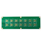
Advanced High Frequency PCBs with ±10% Impedance Control 3/3mil Min Trace 1-4oz Copper

| Place of Origin | China |
|---|---|
| Brand Name | JIETENG |
| Model Number | PCB circuit board |
| Minimum Order Quantity | Negotiable |
| Price | Negotiable |
| Packaging Details | Blank carton, vacuum packed |
| Delivery Time | 5-8 working day |
| Payment Terms | Negotiable |
| Supply Ability | 360000 square meters / year |

Contact me for free samples and coupons.
Whatsapp:0086 18588475571
Wechat: 0086 18588475571
Skype: sales10@aixton.com
If you have any concern, we provide 24-hour online help.
xProduct Details
| Impedance Control | ±10% | Min Trace Width/Space | 3/3mil |
|---|---|---|---|
| Min Hole Size | 0.2mm | Solder Mask Color | Green, Blue, White, Black, Etc. |
| Board Thickness | 0.2-3.2mm | Surface Finish | HASL, ENIG, OSP, Etc. |
| Packaging | Vacuum Packing, Bubble Bag, Carton Box, Etc. | Copper Thickness | 1-4oz |
| High Light | 1-4oz High Frequency PCBs,3/3mil High Frequency PCBs |
||
Product Description
Product Description:
High Frequency Printed Circuit Boards (PCBs) are the backbone of modern electronics, enabling the high-speed and high-performance operation that today's technologies demand. Designed to accommodate the rapid transmission of signals with minimal loss and distortion, these High-Speed Printed Boards are crafted with precision and are optimized for a wide range of applications, including but not limited to, telecommunications, aerospace, and medical equipment. Our High Frequency PCBs boast a range of features and specifications that make them an ideal choice for anyone looking for High-Speed Printed Circuit Boards that deliver reliability and performance.
One of the most critical specifications in High Frequency PCBs is the copper thickness, and our boards come with options ranging from 1oz to 4oz. This variable copper thickness allows for flexibility in design and application, ensuring that whether your project requires minimal or extensive current carrying capacity, our High-Speed Printed Boards can be tailored to meet those needs. This customization allows designers to optimize for power distribution, signal integrity, and thermal management, all of which are crucial for High-Performance Circuit Boards.
Precision is key in circuit design, and our High Frequency PCBs feature a minimum trace width and space of 3/3mil. This fine level of detail ensures that our High-Speed Printed Circuit Boards can support intricate designs without compromise. The tight trace and space capabilities enable more complex and denser circuits, providing the foundation for sophisticated and compact electronic devices. This is particularly beneficial for applications where space is at a premium and performance cannot be sacrificed.
At the heart of any PCB are the vias and through-holes that offer pathways for electrical connectivity across the different layers of the board. Our High Frequency PCBs come with a minimum hole size of 0.2mm, accommodating the industry's need for miniaturization while maintaining functionality and reliability. This small hole size allows for the inclusion of more holes per unit area, which is essential for multi-layer High-Speed Printed Circuit Boards that require complex routing and interconnectivity.
Aesthetics and functionality go hand in hand, and that's why we offer our High Frequency PCBs with a variety of solder mask colors including green, blue, white, black, and more. The solder mask not only protects the copper circuits from environmental factors and potential short-circuits but also provides a professional and customized look to the High-Speed Printed Boards. The variety of colors can be used to differentiate various boards within a system or to align with company branding.
The board thickness is another aspect where our High Frequency PCBs offer versatility, with options ranging from 0.2mm to 3.2mm. This range allows for the creation of both flexible and rigid High-Speed Printed Circuit Boards, accommodating different levels of mechanical stability and flexibility as required by different applications. Whether you need a thin, lightweight board for a portable device or a thick, sturdy board for a high-power application, our High-Performance Circuit Boards can be customized to your specifications.
In conclusion, our High Frequency PCBs are engineered to meet the stringent demands of high-speed and high-performance electronic applications. With features like diverse copper thickness, fine trace width and spacing, small hole sizes, multiple solder mask color options, and a range of board thicknesses, these High-Speed Printed Boards stand out as a premier choice for any project. If you're looking for High-Performance Circuit Boards that will power your next innovation, look no further than our High Frequency PCBs designed for excellence and reliability.
Features:
- Product Name: High Frequency PCBs
- Board Thickness: 0.2-3.2mm
- Silk Screen Color: White, Black, Yellow, Etc.
- Impedance Control: ±10%
- Min Hole Size: 0.2mm
- Layer: 2-10
- High-Speed Printed Boards
- High-Frequency Circuit Boards
Technical Parameters:
| Attribute | Specification |
|---|---|
| Silk Screen Color | White, Black, Yellow, Etc. |
| Solder Mask Color | Green, Blue, White, Black, Etc. |
| Surface Finish | HASL, ENIG, OSP, Etc. |
| Copper Thickness | 1-4oz |
| Material | FR4 |
| Layer | 2-10 |
| Min Hole Size | 0.2mm |
| Board Thickness | 0.2-3.2mm |
| Packaging | Vacuum Packing, Bubble Bag, Carton Box, Etc. |
| Impedance Control | ±10% |
Applications:
The JIETENG brand is synonymous with the cutting-edge technology of High-Speed Printed Circuit Boards , offering a wide range of applications for various high-frequency scenarios. The JIETENG PCB circuit board , with its model number proudly etched into its surface, is a prime example of impeccable engineering and manufacturing prowess originating from China . These boards are specifically designed to cater to industries where precision and reliability are of utmost importance.
With a minimum trace width/space of 3/3mil and a board thickness that can vary from 0.2-3.2mm , the JIETENG boards are versatile and can be customized to fit the requirements of complex electronic assemblies. This versatility makes them ideal for applications ranging from aerospace to telecommunications, where high-speed signal transmission is critical. The JIETENG brand ensures that each High-Frequency Printed Board is built to exceed performance expectations in these demanding environments.
Featuring anywhere from 2-10 layers , these robust PCBs can accommodate the intricate circuitry required for advanced electronic devices. The minimum hole size of 0.2mm further highlights the precision with which these boards are manufactured, allowing for high-density interconnects and superior electrical performance in high-speed applications. The JIETENG High-Speed Printed Boards are thus an integral component in the realm of sophisticated electronics where every millimeter counts.
Packaged meticulously in Vacuum Packing , safeguarded by Bubble Bags , and finally encased in sturdy Carton Boxes , JIETENG ensures that their high-frequency PCBs arrive at their destination in pristine condition, ready for immediate use. Whether it's a high-speed server, a precision medical imaging device, or a communication satellite, the JIETENG High-Frequency Printed Boards are engineered to facilitate peak performance in an array of applications, assuring quality and reliability in every layer.
Customization:
Brand Name: JIETENG
Model Number: PCB circuit board
Place of Origin: China
Layer: 2-10 layers, suitable for High-Speed Circuit Boards
Silk Screen Color: Available in White, Black, Yellow, etc., for clear identification on High-Frequency Printed Circuit Boards
Packaging: Secure Vacuum Packing, Bubble Bag, and Carton Box to ensure safe delivery of High-Speed Circuit Boards
Surface Finish: Options including HASL, ENIG, OSP, etc., for reliable performance of High-Speed Circuit Boards
Min Hole Size: Precision drilling with a minimum hole size of 0.2mm for High-Frequency Printed Circuit Boards
Support and Services:
Our High Frequency PCBs are designed with superior performance in mind, and as part of our commitment to excellence, we offer comprehensive technical support and services for our products. Our support services include an extensive online knowledge base, detailed product documentation, and access to a suite of diagnostic tools to help troubleshoot and optimize your PCBs performance.
To assist with the design and development process, we provide design guidelines, material specifications, and application notes specifically tailored for high-frequency applications. Our experienced technical support team is available to help with design considerations, material choices, and to answer any questions related to the performance and capabilities of our High Frequency PCBs.
In the event that you encounter any issues with your PCBs, our technical support team is equipped to provide you with rapid and efficient solutions. We offer a range of services including failure analysis, rework recommendations, and we can guide you through any necessary repairs or adjustments to ensure your PCBs meet their intended specifications.
For ongoing maintenance and performance optimization, we offer regular updates and upgrades to our product specifications and support resources. We are dedicated to ensuring that your High Frequency PCBs continue to operate at peak performance throughout their life cycle.
We are committed to providing our customers with the highest level of support and service. Our technical support team is dedicated to your success and is always ready to help you get the most out of your High Frequency PCBs.
Packing and Shipping:
Our High Frequency PCBs are meticulously packaged to ensure their integrity and quality during shipping. Each PCB is individually encased in a static-protective bag to safeguard against electrostatic discharge which can damage sensitive electronic components. The boards are then securely placed between foam pads that provide cushioning and prevent movement inside the packaging box.
The exterior of the packaging is constructed from durable, corrugated cardboard that provides structural strength to withstand the rigors of transportation. The box is sealed with heavy-duty packing tape to prevent accidental opening and exposure to environmental elements. A packing list is included on the outside of the box for easy identification and verification upon receipt.
To further ensure the safe delivery of our High Frequency PCBs, we use reputable shipping carriers with tracking capabilities. Customers will receive a tracking number upon dispatch so they can monitor the progress of their shipment until it arrives at its destination. We take every precaution to deliver our High Frequency PCBs promptly and in perfect condition.
FAQ:
Q1: What is a High Frequency PCB and what are its applications?
A1: A High Frequency PCB, manufactured by JIETENG, is a type of PCB circuit board designed to transmit signals over a high frequency range. These PCBs are often used in applications such as advanced communication systems, microwave, radio frequency, and high-speed design applications where signal integrity is paramount.
Q2: What materials are used in the construction of JIETENG High Frequency PCBs?
A2: JIETENG High Frequency PCBs are typically constructed using materials that have low dielectric loss, high thermal conductivity, and stable electrical properties over a wide range of frequencies. Common materials include specialized high-frequency laminates such as PTFE (Teflon), FR4, or proprietary blends that meet the specific performance requirements of the application.
Q3: Can I get a custom High Frequency PCB circuit board designed and manufactured by JIETENG?
A3: Yes, JIETENG offers custom design and manufacturing services for High Frequency PCB circuit boards. Customers can specify their requirements, including dimensions, layer count, material type, impedance control, and other specifications, and JIETENG will provide a PCB tailored to meet those needs.
Q4: How does JIETENG ensure the quality of its High Frequency PCBs?
A4: JIETENG employs a strict quality control process that includes material inspection, design verification, manufacturing process control, and final testing to ensure that all High Frequency PCBs meet the required standards. Additionally, as a manufacturer based in China, JIETENG adheres to both national and international quality and performance standards.
Q5: What is the lead time for ordering a High Frequency PCB from JIETENG?
A5: The lead time for High Frequency PCBs can vary depending on the complexity of the design, order quantity, and material availability. JIETENG works with customers to provide estimated lead times during the ordering process. For specific lead time information, customers should contact JIETENG with their order details.
Recommended Products