


All Products
Contact Person :
Sales Manager
Phone Number :
13510910864
Whatsapp :
+8613360524484
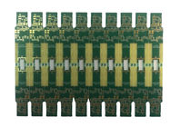
White Silk Screen High Frequency PCBs with FR4 2-10 Layer HASL/ENIG/OSP

| Place of Origin | China |
|---|---|
| Brand Name | JIETENG |
| Model Number | PCB circuit board |
| Minimum Order Quantity | Negotiable |
| Price | Negotiable |
| Packaging Details | Blank carton, vacuum packed |
| Delivery Time | 5-8 working day |
| Payment Terms | Negotiable |
| Supply Ability | 360000 square meters / year |

Contact me for free samples and coupons.
Whatsapp:0086 18588475571
Wechat: 0086 18588475571
Skype: sales10@aixton.com
If you have any concern, we provide 24-hour online help.
xProduct Details
| Material | FR4 | Layer | 2-10 |
|---|---|---|---|
| Surface Finish | HASL, ENIG, OSP, Etc. | Silk Screen Color | White, Black, Yellow, Etc. |
| Min Hole Size | 0.2mm | Board Thickness | 0.2-3.2mm |
| Copper Thickness | 1-4oz | Packaging | Vacuum Packing, Bubble Bag, Carton Box, Etc. |
| High Light | 2-10 Layer High Frequency PCBs,FR4 High Frequency PCBs,White Silk Screen High Frequency PCBs |
||
Product Description
Product Description:
High Frequency PCBs, or High-Speed Printed Boards, are the backbone of modern electronic communication devices. Designed to cater to the demanding requirements of high-speed signal transmission, these boards ensure that electronics can keep up with the rapid pace of technological advancement. Our High-Frequency Printed Circuit Boards are engineered with precision to provide exceptional performance for applications where the integrity of the signal is paramount.
Our High Frequency PCBs come in a variety of layer configurations, ranging from 2 to 10 layers. This flexibility allows for complex, multi-layer designs that are ideal for sophisticated electronic components. Whether you are working on a simple two-layer board or a more intricate ten-layer design, our products are manufactured to meet the highest standards of quality and reliability.
The copper thickness on these boards is another critical factor in their performance. Our High-Speed Printed Boards are available with copper thicknesses ranging from 1oz to 4oz. This variability allows designers to choose the appropriate weight to match the electrical requirements of their projects, ensuring that the boards can handle the necessary current levels and improve the thermal management of the system.
Board thickness is also a key consideration, and our High Frequency PCBs are offered in a range from 0.2mm to 3.2mm. This range accommodates various applications from ultra-thin mobile devices to more robust industrial machinery. The thickness of the board can have a significant impact on its durability, flexibility, and thermal characteristics, making it crucial to select the right specification for your application.
The material used in the construction of these High-Speed Printed Boards is FR4, a well-known and highly reliable substrate in the PCB industry. FR4 is known for its excellent electrical insulation, mechanical strength, and thermal resistance, making it an ideal choice for High-Frequency Printed Circuit Boards that are exposed to demanding operating conditions.
To ensure that our High Frequency PCBs reach you in perfect condition, we employ meticulous packaging standards. Our boards are first vacuum packed to remove any air and prevent oxidation or contamination. Once vacuum-sealed, they are placed in a bubble bag, offering an additional layer of protection against physical shock during transportation. Finally, the packaged boards are securely placed in a sturdy carton box, ensuring that they are well-protected until they reach your doorstep. This combination of packaging materials guarantees that your High Frequency PCBs are delivered to you ready for immediate use and free of any damage.
In summary, our High Frequency PCBs offer an optimal blend of functionality and durability. With customizable layer counts, copper thicknesses, and board thicknesses, along with the reliability of FR4 material, these High-Speed Printed Boards are crafted to support the most demanding high-frequency applications. All of this is complemented by our thorough packaging process, which includes vacuum packing, bubble bagging, and carton boxing to ensure that your High-Frequency Printed Circuit Boards arrive in pristine condition. Whether for telecommunications, aerospace, medical devices, or consumer electronics, our PCBs stand as a testament to our commitment to quality and performance in the high-speed electronics industry.
Features:
- Product Name: High Frequency PCBs
- Solder Mask Color: Green, Blue, White, Black, Etc.
- Packaging: Vacuum Packing, Bubble Bag, Carton Box, Etc.
- Surface Finish: HASL, ENIG, OSP, Etc.
- Layer: 2-10 Layers for High-Speed Printed Circuit Boards
- Min Hole Size: 0.2mm for High-Performance Printed Circuit Boards
Technical Parameters:
| Parameter | Details |
|---|---|
| Silk Screen Color | White, Black, Yellow, Etc. |
| Impedance Control | ±10% |
| Solder Mask Color | Green, Blue, White, Black, Etc. |
| Material | FR4 |
| Packaging | Vacuum Packing, Bubble Bag, Carton Box, Etc. |
| Surface Finish | HASL, ENIG, OSP, Etc. |
| Copper Thickness | 1-4oz |
| Min Hole Size | 0.2mm |
| Min Trace Width/Space | 3/3mil |
| Layer | 2-10 |
Applications:
JIETENG high-frequency circuit boards are specifically designed for applications where the performance of high-speed printed boards is critical to the functionality and reliability of the overall system. These PCB circuit boards, originating from China, are engineered to cater to a wide range of industries and scenarios, ensuring optimal signal integrity and system performance. With a focus on precision, these boards come with an impedance control of ±10%, a minimum hole size of 0.2mm, and a minimum trace width/space of 3/3mil. The surface finish options include HASL, ENIG, OSP, among others, to meet various environmental and assembly requirements. JIETENG's model number PCB circuit board is versatile, with available layers ranging from 2 to 10, to suit the complexity and design needs of different applications.
The use of JIETENG's high-speed circuit boards extends to advanced communication systems, where maintaining the integrity of high-frequency signals is paramount. These systems often require PCBs that can handle gigahertz-range frequencies without significant losses or reflections, which is where the precision of JIETENG's boards becomes invaluable. In the realm of aerospace and defense, reliability and performance are non-negotiable; the JIETENG high-frequency PCBs provide the robustness needed for equipment subjected to extreme conditions while ensuring consistent communication and control signals.
Medical devices also benefit from the specialized attributes of these high-frequency PCBs. Diagnostic equipment such as MRI and ultrasound machines rely on high-speed circuitry to deliver precise imaging and data. The precision and reliability of JIETENG's PCB circuit boards ensure that these life-saving devices operate at their best. Additionally, in the fast-growing field of the Internet of Things (IoT), the need for efficient and robust communication between devices makes high-frequency PCBs an essential component. JIETENG's PCBs facilitate the rapid and reliable transmission of data that smart devices and sensors require to perform optimally in a connected environment.
Moreover, in consumer electronics, where the demand for faster and more reliable devices continues to grow, the use of JIETENG's high-frequency circuit boards can be seen in products such as smartphones, tablets, and high-performance computers. These applications benefit from the PCB's ability to support high-speed data transfer and reduce electromagnetic interference (EMI), which is crucial for maintaining signal clarity in densely packed electronic devices.
In conclusion, the diverse applications of JIETENG's high-frequency PCBs underscore their adaptability and proficiency in meeting the high standards of various high-tech industries. Whether for critical defense systems, advanced medical technologies, cutting-edge consumer electronics, or the intricacies of IoT, JIETENG provides a PCB circuit board solution that is synonymous with excellence and reliability.
Customization:
Brand Name: JIETENG
Model Number: PCB circuit board
Place of Origin: China
Silk Screen Color: Available in a variety of colors including White, Black, Yellow, Etc.
Min Trace Width/Space: Precision crafting with 3/3mil for high-density design requirements.
Board Thickness: A range of 0.2-3.2mm to cater to diverse High-Frequency Circuit Boards applications.
Material: Utilizing FR4 for High-Performance Printed Circuit Boards that demand reliability.
Min Hole Size: As small as 0.2mm for intricate High-Speed Printed Boards designs.
Support and Services:
Our High Frequency PCBs are designed to deliver superior performance in applications where high signal integrity is essential. To ensure that our customers maximize the utility and functionality of our products, we offer comprehensive technical support and services tailored to meet your specific needs.
Technical Support: Our team of experienced engineers is available to provide you with expert advice and assistance. They can help troubleshoot issues, offer guidance on best practices for PCB design, and provide tips for optimizing the performance of your high frequency circuits.
Design Review Service: Before you commit your design to production, our experts can review your PCB layout to identify potential issues that could affect performance at high frequencies. This service helps to ensure that your design is optimized for both manufacturability and functionality.
Material Selection Assistance: The choice of substrate material can significantly impact the performance of High Frequency PCBs. Our specialists can help you select the most appropriate materials for your application to achieve the best possible signal integrity and electrical performance.
Testing and Certification: To ensure the reliability and quality of your High Frequency PCBs, we provide comprehensive testing services. This includes electrical testing, signal integrity analysis, and thermal testing. We can also assist with obtaining the necessary certifications for your industry or application.
After-Sales Support: Our commitment to customer satisfaction extends beyond the sale. We offer ongoing support for our High Frequency PCB products, including assistance with any post-production issues or concerns that may arise.
Documentation and Resources: We provide a wealth of documentation and online resources, including technical datasheets, application notes, and whitepapers, to help you understand and effectively use our High Frequency PCBs.
Custom Solutions: If you have unique requirements or need a customized solution, our engineering team is ready to work with you to develop a High Frequency PCB that meets your specific needs.
Our goal is to ensure that you have all the support and services you need to make your High Frequency PCB project a success. We are committed to providing the highest level of customer service and technical expertise in the industry.
Packing and Shipping:
Our High Frequency PCBs are meticulously packaged to ensure maximum protection during transportation. Each PCB is individually enclosed in anti-static packaging to preserve the integrity of the sensitive electronic components against electrostatic discharge. The boards are then securely placed in a cushioned, rigid box, which is filled with foam or bubble wrap to prevent movement and absorb any shocks that might occur during shipping. We use strong, durable outer cartons that are sealed and labeled according to shipping regulations. We take extra care to make certain that our High Frequency PCBs reach you in perfect working condition.
Before dispatch, every package is thoroughly inspected to verify that it meets our high standards for quality and safety. We also include a packing slip with each shipment, detailing the contents and providing any necessary handling instructions. Our shipping partners have been carefully selected for their reliability and expertise in handling electronic components, ensuring that your High Frequency PCBs are delivered promptly and without damage. Please inspect your shipment upon arrival and contact us immediately if any issues arise. We are committed to customer satisfaction and will address any concerns swiftly.
FAQ:
Q1: What is a High Frequency PCB and what are its typical applications?
A1: A High Frequency PCB, like the JIETENG PCB circuit board, is designed to transmit signals over a high-frequency range, typically exceeding 500 MHz. They are widely used in applications such as microwave, RF and fast speed digital circuits, satellite communication systems, and high-speed data transfer technologies.
Q2: What materials are used in the manufacturing of JIETENG High Frequency PCBs?
A2: JIETENG High Frequency PCBs are typically made with advanced materials that have low dielectric loss and a stable dielectric constant, such as FR4, polyphenylene oxide (PPO) resins, or Teflon. These materials are chosen to ensure minimal signal loss at high frequencies.
Q3: Can the JIETENG PCB circuit board handle outdoor applications?
A3: Yes, the JIETENG PCB circuit board is designed to withstand various environmental conditions and can be used in outdoor applications. It is manufactured under stringent quality control measures in China to ensure reliability and durability in different environments.
Q4: Are the JIETENG High Frequency PCBs customizable according to specific design requirements?
A4: Absolutely, JIETENG offers customization options for their PCB circuit boards. Customers can specify their requirements in terms of size, number of layers, and other specifications to ensure the final product meets their particular design needs.
Q5: How does the JIETENG PCB circuit board ensure signal integrity at high frequencies?
A5: The JIETENG PCB circuit board is engineered with precise impedance control and uses materials with suitable dielectric properties to maintain signal integrity at high frequencies. Moreover, the PCB layout is optimized to reduce signal losses and cross-talk, ensuring reliable performance for high-speed applications.
Recommended Products