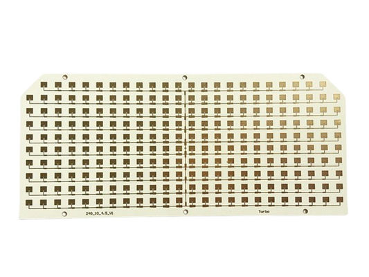
Custom multilayer PCB manufacturing impedance board Rogers 4350 board processing

Contact me for free samples and coupons.
Whatsapp:0086 18588475571
Wechat: 0086 18588475571
Skype: sales10@aixton.com
If you have any concern, we provide 24-hour online help.
x| Solder Mask Color | Green, Blue, White, Black, Red, Etc. | Layer Count | 2-20 |
|---|---|---|---|
| Min. Hole Size | 0.2mm | Surface Finish | HASL, ENIG, OSP, Immersion Silver, Immersion Tin, Etc. |
| Silkscreen Color | White, Black, Yellow, Etc. | Copper Thickness | 1-4oz |
| Board Thickness | 0.2-3.2mm | Min. Line Spacing | 0.1mm |
| Highlight | Custom multilayer PCB manufacturing,Rogers 4350 Custom multilayer PCB,Custom multilayer PCB processing |
||
Product Description:
The Multi-Layer PCB Fabrication product is a cornerstone in the electronics manufacturing industry, offering an advanced solution for sophisticated circuit designs. This product is tailored to meet the needs of high-performance electronics that require reliable and durable circuitry. It is an ideal choice for a wide range of applications including consumer electronics, medical devices, aerospace components, and automotive systems, where multiple layers of circuitry must be precisely aligned and laminated to function as intended.
Our Multi-Layer PCB Manufacturing process utilizes a variety of materials to cater to specific application requirements and to ensure optimal performance under various operating conditions. The materials we offer include standard FR4, High TG FR4 for enhanced thermal resistance, Halogen Free for eco-friendly solutions, and Rogers for high-frequency applications. These materials are selected to provide the best foundation for your PCB, balancing cost, performance, and environmental considerations.
One of the critical aspects of our Multi-Layer PCB Manufacturing is our capability to achieve a minimum line spacing of 0.1mm. This precision allows for higher density of traces and hence, more complex and compact designs. Such fine line spacing is essential for modern electronic devices that require a large number of connections within a limited space, without compromising the signal integrity or electrical performance.
The surface finish of a PCB plays a vital role in its functionality and longevity. Our product offerings include a variety of surface finishes such as HASL (Hot Air Solder Leveling), ENIG (Electroless Nickel Immersion Gold), OSP (Organic Solderability Preservatives), Immersion Silver, and Immersion Tin. Each of these finishes offers different benefits in terms of cost, solderability, shelf life, and electrical characteristics, enabling customers to select the most appropriate finish for their specific application.
Another key attribute of our Multi-Layer PCB Fabrication service is the board thickness range, which spans from 0.2mm to 3.2mm. This range of thicknesses allows for flexibility in design and application. Thinner boards are often used in portable electronics where space is at a premium, while thicker boards may be used in more robust applications where additional strength is required or where the board must support heavier components.
In addition to board thickness, copper thickness is another crucial parameter. Our PCBs are available with copper thicknesses ranging from 1oz to 4oz. The choice of copper thickness impacts the current-carrying capacity of the traces as well as the thermal management of the board. Higher copper thicknesses are typically used in high-power applications or where the PCB needs to dissipate significant amounts of heat.
As part of our comprehensive service, we also offer Multi-Layer PCB Component Assembly. This service streamlines the manufacturing process and allows our customers to receive fully assembled PCBs ready for immediate use in their products. Our assembly services are equipped to handle the latest component packages and are compliant with industry-standard protocols. By integrating component assembly with PCB fabrication, we can reduce the turnaround time and simplify the supply chain for our clients.
In conclusion, our Multi-Layer PCB Fabrication product is designed to meet the highest standards of quality and reliability. With a wide range of materials, fine line spacing, various surface finishes, and a broad spectrum of board and copper thicknesses, we stand ready to support the most demanding electronic projects. Our addition of Multi-Layer PCB Component Assembly services further enhances our offering, making us a one-stop-shop for all your PCB needs. Trust us to bring your electronic concepts to life with precision and efficiency.
Features:
- Product Name: Multilayer PCB Fabrication
- Impedance Control: Yes
- Material: FR4, High TG FR4, Halogen Free, Rogers, etc.
- Min. Hole Size: 0.2mm
- Layer Count: 2-20 layers
- Min. Line Spacing: 0.1mm
- Multi-Level Printed Wiring Board Creation
- Multi-Layer PCB Manufacturing
Technical Parameters:
| Attribute | Specification |
|---|---|
| Min. Line Spacing | 0.1mm |
| Material | FR4, High TG FR4, Halogen Free, Rogers, Etc. |
| Layer Count | 2-20 |
| Min. Line Width | 0.1mm |
| Surface Finish | HASL, ENIG, OSP, Immersion Silver, Immersion Tin, Etc. |
| Copper Thickness | 1-4oz |
| Board Thickness | 0.2-3.2mm |
| Min. Hole Size | 0.2mm |
| Impedance Control | Yes |
| Solder Mask Color | Green, Blue, White, Black, Red, Etc. |
Applications:
The JIETENG PCB circuit board represents the pinnacle of Multi-Level Printed Circuit Board Fabrication , meticulously crafted to meet the rigorous standards of the electronics industry. Originating from China, this model showcases an advanced level of precision with a minimum line width of a mere 0.1mm, allowing for complex and dense circuit designs that are essential in today’s miniaturized electronic components.
Constructed from premium materials such as FR4, High TG FR4, Halogen Free, Rogers, and others, the JIETENG PCB ensures reliability and performance across a multitude of applications. The variety of materials available allows for tailored electrical properties, thermal management, and mechanical stability, making the board suitable for a wide range of operating environments.
With surface finishes including HASL, ENIG, OSP, Immersion Silver, and Immersion Tin, the JIETENG brand caters to different product needs such as enhancing solderability, preventing oxidation, and ensuring wire bondability. These finishes also contribute to the longevity and durability of the Multi-Level Printed Wiring Board Creation , ensuring that the product can withstand the test of time even under strenuous conditions.
Board thickness ranges from 0.2mm to 3.2mm, providing flexibility in design and application. Whether it is for lightweight, portable devices or for more robust, stationary technology, JIETENG's PCB can be adapted to fit the specific needs of the product. The precise control over board thickness also benefits multilayer configurations, which are a staple in complex electronic assemblies.
Impedance control is another critical feature of the JIETENG PCB, ensuring that signal integrity is maintained across the circuit. This is particularly important for high-speed electronic devices where consistent impedance is paramount for maintaining performance and avoiding signal reflection and loss.
Applications of the JIETENG Multi-Level Printed Circuit Board Fabrication are vast and varied. They are commonly used in high-reliability sectors such as aerospace, military, and medical devices, where the utmost precision and quality are non-negotiable. Additionally, they find applications in consumer electronics, telecommunications, automotive industries, and more, where multilevel PCBs are becoming increasingly necessary due to the growing complexity of electronic circuits.
In conclusion, the JIETENG model of PCB circuit boards stands as a testament to the brand's commitment to excellence in Multi-Level Printed Circuit Board Fabrication . Its combination of material quality, fine line precision, varied surface finishes, and stringent impedance control make it an ideal choice for a multitude of scenarios where performance and reliability are essential.
Customization:
Brand Name: JIETENG
Model Number: PCB circuit board
Place of Origin: China
Layer Count: 2-20 layers, accommodating a variety of Multi-Level Printed Wiring Board Creation needs
Board Thickness: Ranging from 0.2 to 3.2mm, our Multi-Layer Printed Circuit Board Production services ensure versatility and durability
Min. Hole Size: Precision drilling with a minimum hole size of 0.2mm
Impedance Control: Yes, to guarantee signal integrity across all Multi-Level Printed Wiring Board Creation applications
Silkscreen Color: Customizable with options including White, Black, Yellow, and more to meet your specific Multi-Layer Printed Circuit Board Production requirements
Support and Services:
Our Multilayer PCB Fabrication service includes comprehensive technical support and a range of services to ensure the highest quality and performance of your multilayer printed circuit boards. Our dedicated team of experts provides assistance at every step, from design and layout optimization to manufacturing and post-production testing. We offer design guideline consultations to help you avoid common pitfalls and ensure manufacturability.
Our services include detailed DFM (Design for Manufacturability) checks, which are essential for multilayer PCBs due to their complexity. We also provide impedance control advice and stack-up recommendations to meet your specific application needs. With state-of-the-art equipment and advanced processes, we ensure precise layer alignment and reliable interlayer connections.
For quality assurance, we conduct thorough inspections and various tests, including electrical testing, microsection analysis, and solderability tests, to guarantee that each PCB meets the highest standards. In the event of any issues or defects, we have a responsive support team ready to assist you with troubleshooting and resolving any problems promptly.
We are committed to supporting you throughout the lifecycle of your product. Our support extends beyond delivery, with services like technical consultations for future revisions and design iterations. We strive to build long-term partnerships by providing exceptional service and technical expertise for all your multilayer PCB fabrication needs.
Packing and Shipping:
The Multilayer PCB (Printed Circuit Board) Fabrication product is meticulously packaged to ensure its integrity and quality during shipping. Each PCB is first individually enclosed in a static-protective bag to safeguard against electrostatic discharge that could damage the circuitry. These bags are then securely placed within cushioned packaging materials that provide ample protection against physical shock and vibration.
The cushioned PCBs are then arranged in a sturdy, corrugated cardboard box, which is custom-sized to prevent excess movement during transit. The box is sealed with strong packing tape and clearly labeled with "Fragile - Handle with Care" to instruct handlers on the careful management of the package. For added security, the shipment includes a packing list that verifies the contents and allows for easy identification upon arrival.
Before dispatch, the entire package is weighed and measured to ensure compliance with carrier regulations and to determine the most efficient and cost-effective shipping method. The shipping label with a tracking number is affixed to the package, enabling both the sender and recipient to monitor the progress of the shipment until its safe delivery. Our commitment to excellence in packaging and shipping guarantees that your Multilayer PCB Fabrication product arrives in pristine condition, ready for use.
FAQ:
Q1: What materials are used in the JIETENG PCB circuit boards?
A1: JIETENG PCB circuit boards are manufactured using high-quality materials that typically include FR-4, metal cores for heat dissipation, and various other substrates depending on the specific application requirements. Each layer is carefully selected to ensure optimal performance and reliability.
Q2: What layer counts are available for the JIETENG multilayer PCBs?
A2: JIETENG offers a wide range of layer counts for their multilayer PCBs, which can vary depending on the complexity and requirements of the electronic device. Customers can request customized layer counts to suit their specific needs.
Q3: Can JIETENG PCB circuit boards be used for high-frequency applications?
A3: Yes, JIETENG PCB circuit boards are designed to perform well in high-frequency applications. Specialized materials and design considerations are implemented to ensure signal integrity and reduce electromagnetic interference in high-frequency environments.
Q4: How does JIETENG ensure the quality of its PCB circuit boards?
A4: JIETENG adheres to strict quality control standards throughout the manufacturing process. This includes using state-of-the-art equipment, conducting thorough inspections at each stage of production, and performing various tests to ensure that each PCB circuit board meets the high-quality standards expected by our customers.
Q5: Are JIETENG PCB circuit boards customizable according to specific design requirements?
A5: Absolutely, JIETENG offers custom PCB fabrication services. Customers can provide their specific design requirements, including shape, size, layer count, and material specifications, and JIETENG will tailor the PCB circuit boards to meet those precise needs.


